SBOS235F March 2002 – April 2018 OPA2357 , OPA357
PRODUCTION DATA.
- 1 Features
- 2 Applications
- 3 Description
- 4 Revision History
- 5 Pin Configuration and Functions
- 6 Specifications
-
7 Detailed Description
- 7.1 Overview
- 7.2 Functional Block Diagram
- 7.3
Feature Description
- 7.3.1 OPAx357 Comparison
- 7.3.2 Operating Voltage
- 7.3.3 Enable Function
- 7.3.4 Rail-to-Rail Input
- 7.3.5 Rail-to-Rail Output
- 7.3.6 Output Drive
- 7.3.7 Video
- 7.3.8 Wideband Video Multiplexing
- 7.3.9 Driving Analog-to-Digital Converters
- 7.3.10 Capacitive Load and Stability
- 7.3.11 Wideband Transimpedance Amplifier
- 7.4 Device Functional Modes
- 8 Application and Implementation
- 9 Power Supply Recommendations
- 10Layout
- 11Device and Documentation Support
- 12Mechanical, Packaging, and Orderable Information
Package Options
Mechanical Data (Package|Pins)
- DGS|10
Thermal pad, mechanical data (Package|Pins)
Orderable Information
8.2.2 High-Impedance Sensor Interface
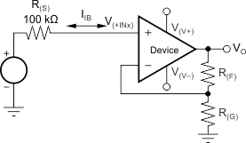
Many sensors have high source impedances that can range up to 10 MΩ, or even higher. The output signal of sensors often must be amplified or otherwise conditioned by an amplifier. The input bias current of this amplifier can load the sensor output and cause a voltage drop across the source resistance, as shown in Figure 44, where (V(+INx) = VS – I(BIAS) × R(S)). The last term, I(BIAS) × R(S), shows the voltage drop across R(S). To prevent errors introduced to the system as a result of this voltage, use an op amp with low input bias current and high-impedance sensors. This low current keeps the error contribution by I(BIAS) × R(S) less than the input voltage noise of the amplifier, so that the amplifier does not become the dominant noise factor. The OPAx357 family of devices series of op amps feature low input bias current (typically 200 fA), and are therefore designed for such applications.
 Figure 44. Noise as a Result of I(BIAS)