SBOS235F March 2002 – April 2018 OPA2357 , OPA357
PRODUCTION DATA.
- 1 Features
- 2 Applications
- 3 Description
- 4 Revision History
- 5 Pin Configuration and Functions
- 6 Specifications
-
7 Detailed Description
- 7.1 Overview
- 7.2 Functional Block Diagram
- 7.3
Feature Description
- 7.3.1 OPAx357 Comparison
- 7.3.2 Operating Voltage
- 7.3.3 Enable Function
- 7.3.4 Rail-to-Rail Input
- 7.3.5 Rail-to-Rail Output
- 7.3.6 Output Drive
- 7.3.7 Video
- 7.3.8 Wideband Video Multiplexing
- 7.3.9 Driving Analog-to-Digital Converters
- 7.3.10 Capacitive Load and Stability
- 7.3.11 Wideband Transimpedance Amplifier
- 7.4 Device Functional Modes
- 8 Application and Implementation
- 9 Power Supply Recommendations
- 10Layout
- 11Device and Documentation Support
- 12Mechanical, Packaging, and Orderable Information
Package Options
Mechanical Data (Package|Pins)
- DGS|10
Thermal pad, mechanical data (Package|Pins)
Orderable Information
7.3.6 Output Drive
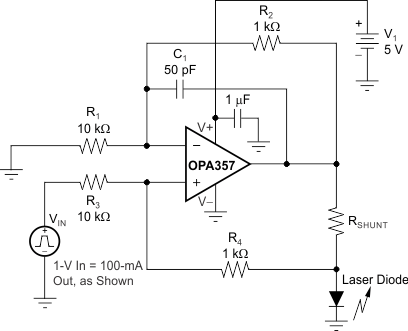
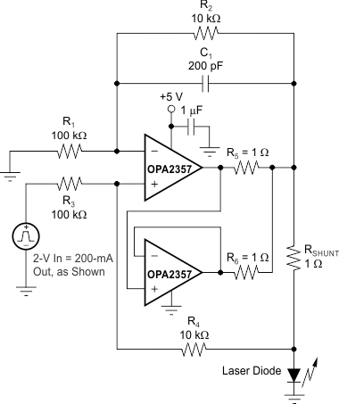
The OPA357 output stage can supply a continuous output current of ±100 mA and still provide approximately 2.7 V of output swing on a 5-V supply, as shown in Figure 33. For maximum reliability, TI recommends running a continuous DC current in excess of ±100 mA; see Figure 21 and Figure 23. For supplying continuous output currents greater than ±100 mA, the OPA357 can be operated in parallel as shown in Figure 34.
The OPA357 provides peak currents up to 200 mA, which corresponds to the typical short-circuit current. Therefore, an on-chip thermal shutdown circuit is provided to protect the OPA357 from dangerously high junction temperatures. At 160°C, the protection circuit shuts down the amplifier. Normal operation resumes when the junction temperature cools to below 140°C.
 Figure 33. Laser Diode Driver
 Figure 34. Parallel Operation