SBOS365G may   2006  – may 2023 OPA2365 , OPA365

PRODUCTION DATA  

  1.   1
  2. Features
  3. Applications
  4. Description
  5. Revision History
  6. Device Comparison Table
  7. Pin Configuration and Functions
  8. Specifications
    1. 7.1 Absolute Maximum Ratings
    2. 7.2 ESD Ratings
    3. 7.3 Recommended Operating Conditions
    4. 7.4 Thermal Information: OPA365
    5. 7.5 Thermal Information: OPA2365
    6. 7.6 Electrical Characteristics
    7. 7.7 Typical Characteristics
  9. Detailed Description
    1. 8.1 Overview
    2. 8.2 Functional Block Diagram
    3. 8.3 Feature Description
      1. 8.3.1 Rail-to-Rail Input
      2. 8.3.2 Input and ESD Protection
      3. 8.3.3 Capacitive Loads
      4. 8.3.4 Achieving an Output Level of Zero Volts (0 V)
      5. 8.3.5 Active Filtering
    4. 8.4 Device Functional Modes
  10. Application and Implementation
    1. 9.1 Application Information
      1. 9.1.1 Basic Amplifier Configurations
    2. 9.2 Typical Application
      1. 9.2.1 Design Requirements
      2. 9.2.2 Detailed Design Procedure
      3. 9.2.3 Application Curve
    3. 9.3 System Examples
      1. 9.3.1 Driving an Analog-to-Digital Converter
    4. 9.4 Power Supply Recommendations
    5. 9.5 Layout
      1. 9.5.1 Layout Guidelines
      2. 9.5.2 Layout Example
  11. 10Device and Documentation Support
    1. 10.1 Device Support
      1. 10.1.1 Development Support
        1. 10.1.1.1 PSpice® for TI
        2. 10.1.1.2 TINA-TI™ Simulation Software (Free Download)
        3. 10.1.1.3 DIP-Adapter-EVM
        4. 10.1.1.4 DIYAMP-EVM
        5. 10.1.1.5 TI Reference Designs
        6. 10.1.1.6 Filter Design Tool
    2. 10.2 Documentation Support
      1. 10.2.1 Related Documentation
    3. 10.3 Receiving Notification of Documentation Updates
    4. 10.4 Support Resources
    5. 10.5 Trademarks
    6. 10.6 Electrostatic Discharge Caution
    7. 10.7 Glossary
  12. 11Mechanical, Packaging, and Orderable Information

Package Options

Mechanical Data (Package|Pins)
Thermal pad, mechanical data (Package|Pins)
Orderable Information

Rail-to-Rail Input

The OPAx365 product family features true rail-to-rail input operation, with supply voltages as low as ±1.1 V
(2.2 V). A unique zerø-crossover input topology eliminates the input offset transition region typical of many rail-to-rail, complementary stage operational amplifiers. This topology also allows the OPAx365 to provide excdellent common-mode performance over the entire input range, which extends 100 mV beyond both power-supply rails, as shown in Figure 8-1. When driving ADCs, the highly linear VCM range of the OPAx365 makes sure that the op amp or ADC system linearity performance is not compromised.
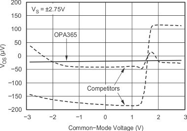
GUID-A9A10700-4AC2-4394-B246-DD952FB947A1-low.gifFigure 8-1 OPA365 Linear Offset Over the Entire Common-Mode Range

For a simplified schematic illustrating the rail-to-rail input circuitry, see Section 8.2.