SBOS075A September 2000 – June 2024 OPA2241 , OPA2251 , OPA241 , OPA251 , OPA4241 , OPA4251
PRODUCTION DATA
- 1
- 1Features
- 2Applications
- 3Description
- 4Pin Configuration and Functions
-
5Specifications
- 5.1 Absolute Maximum Ratings
- 5.2 Recommended Operating Conditions
- 5.3 Thermal Information for OPA241 and OPA251
- 5.4 Thermal Information for OPA2241 and OPA2251
- 5.5 Thermal Information for OPA4241 and OPA4251
- 5.6 Electrical Characteristics for VS = 2.7V to 5V
- 5.7 Electrical Characteristics for VS = ±15V
- 5.8 Typical Characteristics
- 6Application and Implementation
- 7Device and Documentation Support
- 8Revision History
- 9Mechanical, Packaging, and Orderable Information
Package Options
Refer to the PDF data sheet for device specific package drawings
Mechanical Data (Package|Pins)
- D|8
- P|8
Thermal pad, mechanical data (Package|Pins)
Orderable Information
6.1.3 Capacitive Load and Stability
The OPAx241 series and OPAx251 series can drive a wide range of capacitive loads. However, all op amps under certain conditions can be unstable. Op amp configuration, gain, and load value are just a few of the factors to consider when determining stability.
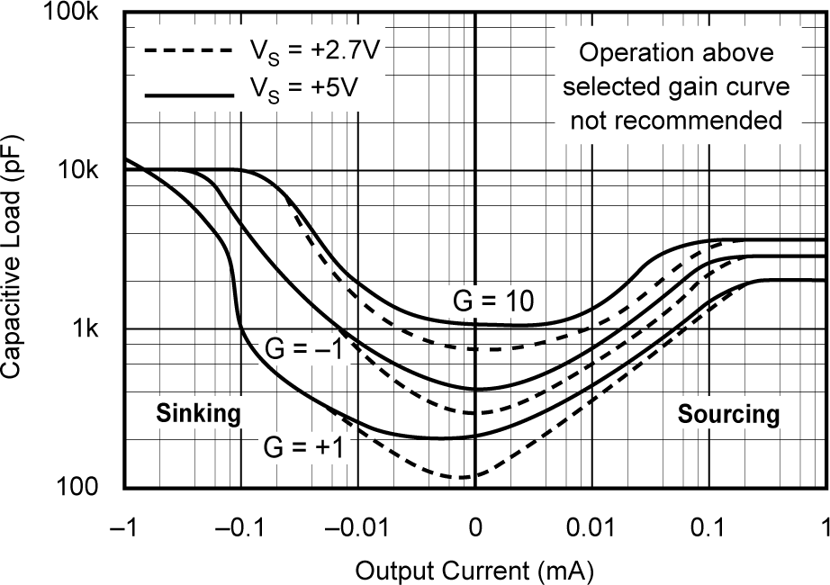
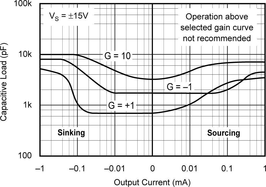
Figure 6-2 and Figure 6-3 show the regions where the OPAx241 series and OPAx251 series have the potential for instability. As shown, the unity gain configuration with low supplies is the most susceptible to the effects of capacitive load. With VS = 5V, G = 1, and IOUT = 0, operation remains stable with load capacitance up to approximately 200pF. Increasing a combination of supply voltage, output current, and gain significantly improves capacitive load drive. For example, increasing the supplies to ±15V and gain to 10 drives approximately 2700pF.
Figure 6-4 shows one method to improve capacitive load drive in the unity gain configuration by inserting a resistor inside the feedback loop. This reduces ringing with large capacitive loads while maintaining dc accuracy. For example, with VS = ±1.35V and RS = 5kΩ, the OPAx241 series and OPAx251 series perform well with capacitive loads in excess of 1000pF. Without the series resistor, the capacitive load drive is typically 200pF for these conditions. However, this method results in a slight reduction of output voltage swing.
 Figure 6-2 Stability—Capacitive Load vs Output Current
for Low Supply Voltage
 Figure 6-3 Stability—Capacitive Load vs Output Current
for ±15V Supplies
 Figure 6-4 Series Resistor in Unity Gain
Configuration Improves Capacitive Load Drive
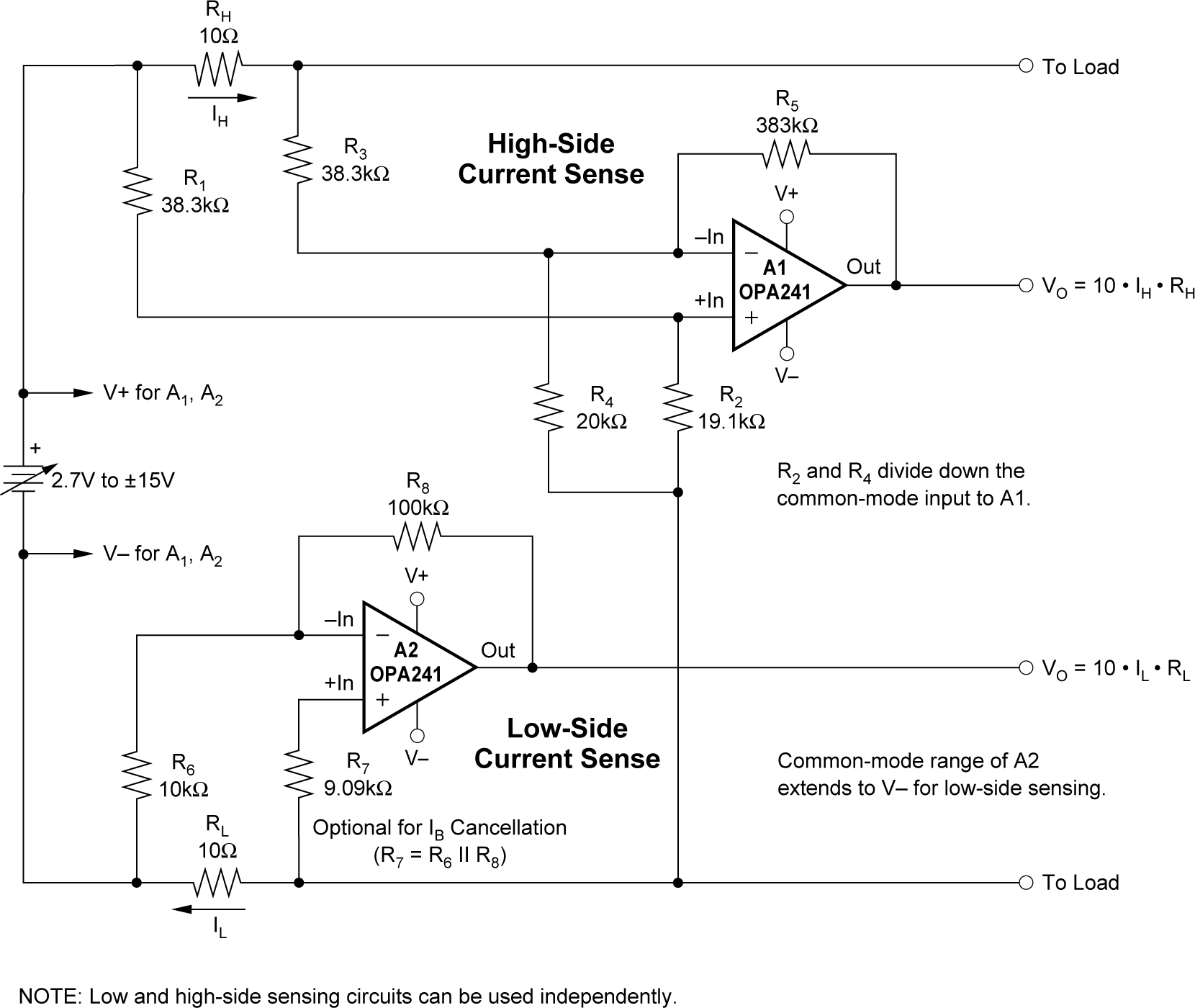
 Figure 6-5 Low-Side and High-Side Battery Current
Sensing