SBOS981J October 2019 – April 2021 OPA2607 , OPA607
PRODUCTION DATA
- 1 Features
- 2 Applications
- 3 Description
- 4 Revision History
- 5 Device Comparison
- 6 Pin Configuration and Functions
- 7 Specifications
- 8 Detailed Description
- 9 Application and Implementation
- 10Power Supply Recommendations
- 11Layout
- 12Device and Documentation Support
- 13Mechanical, Packaging, and Orderable Information
Package Options
Mechanical Data (Package|Pins)
Thermal pad, mechanical data (Package|Pins)
- RUG|10
Orderable Information
8.3.3 Input and ESD Protection
When the primary design goal is a linear amplifier with high CMRR, do not exceed the op amp input common-mode voltage range (VCM). This CMRR is used to set the common-mode input range specifications in Section 7.5. The typical VCM specifications for the OPAx607 devices are from the negative rail to 1.1 V below the positive rail. Assuming the op amp is in linear operation, the voltage difference between the input pins is small (ideally 0 V) and the input common-mode voltage can be analyzed at either input pin; the other input pin is assumed to be at the same potential. The voltage at VIN+ is easy to evaluate. In a noninverting configuration (Figure 8-1) the input signal, VIN+, must not exceed the VCM rating. However, in an inverting amplifier configuration, VIN+ must be connected to the voltage within VCM. The input signal applied at VIN- can be any voltage, such that the output voltage swings with a headroom of 10 mV from either of the supply rails.
The input voltage limits have fixed headroom to the power rails and track the power-supply voltages. For single 5-V supply, the linear input voltage range is 0 V to 3.9 V and with a 2.2-V supply this range is 0 V to 1.1 V. The headroom to each power-supply rail is the same in either case: 0 V and 1.1 V. A weak NMOS input pair from VIN+ to VIN+ – 1.1 V ensures that an output phase reversal issue does not occur when the VCM is violated.
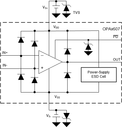
 Figure 8-4 Internal ESD Structure
The OPAx607 devices also incorporate internal electrostatic discharge (ESD) protection circuits on all pins. For the input and output pins, this protection primarily consists of current-steering diodes connected between the input and power-supply pins. These ESD protection diodes provides input overdrive protection, as long as the current is limited with a series resistor to 10 mA, as stated in Section 7.1. Figure 8-1 shows a series input resistor can be added to the driven input to limit the input current.