SBOS079C March   1999  – February 2023 OPA2277 , OPA277 , OPA4277

PRODUCTION DATA  

  1. Features
  2. Applications
  3. Description
  4. Revision History
  5. Pin Configuration and Functions
  6. Specifications
    1. 6.1 Absolute Maximum Ratings
    2. 6.2 ESD Ratings
    3. 6.3 Recommended Operating Conditions
    4. 6.4 Thermal Information: OPA277
    5. 6.5 Thermal Information: OPA2277
    6. 6.6 Thermal Information: OPA4277
    7. 6.7 Electrical Characteristics
    8. 6.8 Typical Characteristics
  7. Detailed Description
    1. 7.1 Overview
    2. 7.2 Functional Block Diagram
    3. 7.3 Feature Description
      1. 7.3.1 Operating Voltage
      2. 7.3.2 Offset Voltage Adjustment
      3. 7.3.3 Input Protection
      4. 7.3.4 Input Bias Current Cancellation
      5. 7.3.5 EMI Rejection Ratio (EMIRR)
        1. 7.3.5.1 EMIRR IN+ Test Configuration
    4. 7.4 Device Functional Modes
  8. Application and Implementation
    1. 8.1 Application Information
    2. 8.2 Typical Applications
      1. 8.2.1 Second-Order, Low-Pass Filter
        1. 8.2.1.1 Design Requirements
        2. 8.2.1.2 Detailed Design Procedure
        3. 8.2.1.3 Application Curve
      2. 8.2.2 Load Cell Amplifier
      3. 8.2.3 Thermocouple Low-Offset, Low-Drift Loop Measurement With Diode Cold Junction Compensation
    3. 8.3 Power Supply Recommendations
    4. 8.4 Layout
      1. 8.4.1 Layout Guidelines
        1. 8.4.1.1 DRM Package (8-Pin VSON)
      2. 8.4.2 Layout Example
  9. Device and Documentation Support
    1. 9.1 Device Support
      1. 9.1.1 Development Support
        1. 9.1.1.1 PSpice® for TI
        2. 9.1.1.2 TINA-TI™ Simulation Software (Free Download)
        3. 9.1.1.3 DIP-Adapter-EVM
        4. 9.1.1.4 DIYAMP-EVM
        5. 9.1.1.5 TI Reference Designs
        6. 9.1.1.6 Filter Design Tool
    2. 9.2 Documentation Support
      1. 9.2.1 Related Documentation
    3. 9.3 Receiving Notification of Documentation Updates
    4. 9.4 Support Resources
    5. 9.5 Trademarks
    6. 9.6 Electrostatic Discharge Caution
    7. 9.7 Glossary
  10. 10Mechanical, Packaging, and Orderable Information

Package Options

Refer to the PDF data sheet for device specific package drawings

Mechanical Data (Package|Pins)
  • D|8
  • DRM|8
  • P|8
Thermal pad, mechanical data (Package|Pins)
Orderable Information

Typical Characteristics

At TA = 25°C, VS = ±15 V, and RL = 2 kΩ, unless otherwise noted.
GUID-F3256596-C9EC-415C-8D9A-E9FA5EEB0D16-low.gif
 
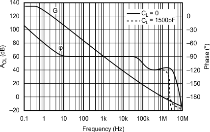
Figure 6-1 Open-Loop Gain and Phase vs Frequency
GUID-71D2604D-DC70-48A8-8393-AE330400E0A4-low.gif
 
Figure 6-3 Input Noise and Current Noise Spectral Density vs Frequency
GUID-763D527B-76E2-4085-B793-753874752DE2-low.gif
 
Figure 6-5 Channel Separation vs Frequency
GUID-3AF41CAF-C4EF-48AE-AABB-68EBDA128764-low.gif
 
Figure 6-7 Offset Voltage Production Distribution
GUID-BD1A1364-14EA-436F-844E-E73E888ADB83-low.gif
 
Figure 6-9 Warm-Up Offset Voltage Drift
GUID-9B229130-32F3-4578-BF3E-55467ED030FD-low.gif
 
Figure 6-11 Input Bias Current vs Temperature
GUID-4BA9811F-84AE-4003-B515-ADA8751BBB56-low.gif
 
Figure 6-13 Change in Input Bias Current vs Power-Supply Voltage
GUID-9B3BAB5F-8373-4CA5-9D80-B47A6047580D-low.gif
 
Figure 6-15 Quiescent Current vs Supply Voltage
GUID-3E959938-38AC-4756-8BF7-242CEBE3D4D8-low.gif
 
Figure 6-17 Maximum Output Voltage vs Frequency
GUID-7D2CEC44-18B4-40C0-8D7A-B8E027F3A7E7-low.gif
 
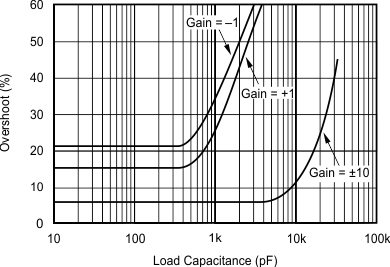
Figure 6-19 Small-Signal Overshoot vs Load Capacitance
GUID-58BD845A-0112-439C-8F82-886C578E3E4C-low.gif
G = 1, CL = 0, VS = ±15 V
Figure 6-21 Small-Signal Step Response
GUID-544091EA-A728-4056-970F-9BA5E12C644C-low.gif
VS = ±15 V
Figure 6-23 Open-Loop Output Impedance
GUID-8811E8DB-9801-4AF2-9E6A-0B648C1B9214-low.gif
 
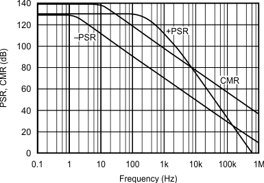
Figure 6-2 Power Supply and Common-Mode Rejection vs Frequency
GUID-DEF1F0F2-8B57-4805-8AFB-C3897DC7F40A-low.gif
 
Figure 6-4 Input Noise Voltage vs Time
GUID-7072BE3E-3A15-4C4F-A937-B1CD57F0381D-low.gif
 
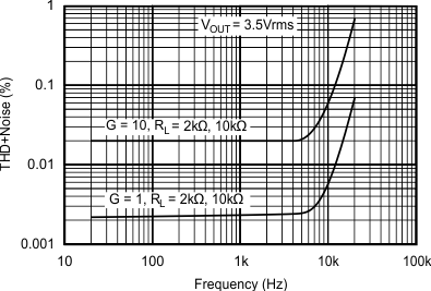
Figure 6-6 Total Harmonic Distortion + Noise vs Frequency
GUID-B713BF5B-44A1-494B-A329-F4F98290073C-low.gif
 
Figure 6-8 Offset Voltage Drift Production Distribution
GUID-962B2BC3-8CF5-46C8-ADC2-1DE6A12D5012-low.gif
 
Figure 6-10 AOL, CMR, PSR vs Temperature
GUID-2926D5FE-75F5-4A32-987D-51E91586C544-low.gif
 
Figure 6-12 Quiescent Current and Short-Circuit Current vs Temperature
GUID-949BF739-5212-4D85-95CC-BA314F808B80-low.gif
 
Figure 6-14 Change in Input Bias Current vs Common-Mode Voltage
GUID-6F8E5818-8B67-40B7-895B-EF5D3FBB3294-low.gif
 
Figure 6-16 Settling Time vs Closed-Loop Gain
GUID-41BDAE32-441B-4D97-BDD4-EB1D449E795E-low.gif
 
Figure 6-18 Output Voltage Swing vs Output Current
GUID-9F1E73AE-6A72-4793-A073-DC9931085F86-low.gif
G = 1, CL = 1500 pF, VS = ±15 V
Figure 6-20 Large-Signal Step Response
GUID-40422087-E6C8-4FC9-98DC-80640D602B8A-low.gif
G = 1, CL = 1500 pF, VS = ±15 V
Figure 6-22 Small-Signal Step Response