SBOS671D September 2018 – December 2022 OPA2828 , OPA828
PRODUCTION DATA
- 1 Features
- 2 Applications
- 3 Description
- 4 Revision History
- 5 Pin Configuration and Functions
- 6 Specifications
-
7 Detailed Description
- 7.1 Overview
- 7.2 Functional Block Diagram
- 7.3
Feature Description
- 7.3.1 Phase-Reversal Protection
- 7.3.2 Electrical Overstress
- 7.3.3 MUX Friendly Inputs
- 7.3.4 Overload Power Limiter
- 7.3.5 Noise Performance
- 7.3.6 Capacitive Load and Stability
- 7.3.7 Settling Time
- 7.3.8 Slew Rate
- 7.3.9 Full-Power Bandwidth
- 7.3.10 Small-Signal Response
- 7.3.11 Thermal Shutdown
- 7.3.12 Low Offset Voltage Drift
- 7.3.13 Overload Recovery
- 7.4 Device Functional Modes
- 8 Application and Implementation
- 9 Device and Documentation Support
- 10Mechanical, Packaging, and Orderable Information
Package Options
Mechanical Data (Package|Pins)
- DGN|8
Thermal pad, mechanical data (Package|Pins)
- DGN|8
Orderable Information
7.3.3 MUX Friendly Inputs
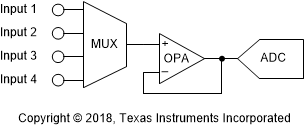
Multiplexing is a frequently-used technique to perform data acquisition in multichannel systems with minimal signal-chain requirements. In this context, the role of the multiplexer (MUX) in an acquisition system is to switch between channels and send each signal as fast as possible to a single data converter, maximizing system throughput and minimizing delay. To provide accurate processing, a precision amplifier is placed downstream from the multiplexer to precisely drive the analog-to-digital converter (ADC). Figure 7-4 illustrates this concept.
 Figure 7-4 Typical
Multiplexed System Block Diagram
Figure 7-4 Typical
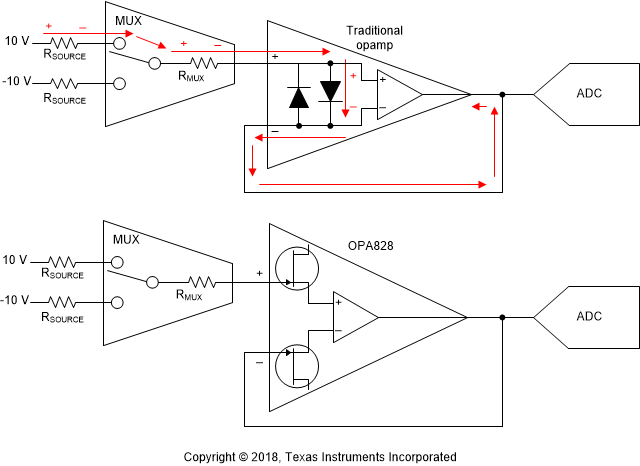
Multiplexed System Block DiagramIn a typical multiplexed application, large transient voltages can often be presented to the input of the op amp driving the ADC. Large input differential voltages are commonly seen during slewing or open-loop operation, which is especially common when switching from one MUX input to another. Traditional precision amplifiers often consist of a differential transistor pair that is protected from large differential transient input voltages with antiparallel diodes between the inputs of the amplifier. These antiparallel diodes are effective at limiting the voltage differential between the inputs to one or two forward diode voltage drops, which protects the precision input devices from damage. However, the antiparallel diodes do have considerable drawbacks such as large inrush currents when turned on. If passive filtering or high source impedance is present, large inrush current can disturb settling time, limiting the throughput of the system and degrading signal-chain precision. The OPAx828 do not need antiparallel diodes to protect the input JFET transistors and are free from large inrush currents, even with differential input voltages as large as ±18 V. These concepts are illustrated in Figure 7-5.
 Figure 7-5 Typical
Multiplexed System Block Diagram