SBOS309E August 2004 – December 2024 OPA2830
PRODUCTION DATA
- 1
- 1 Features
- 2 Applications
- 3 Description
- 4 Device Comparison Table
- 5 Pin Configurations and Functions
-
6 Specifications
- 6.1 Absolute Maximum Ratings
- 6.2 ESD Ratings
- 6.3 Recommended Operating Conditions
- 6.4 Thermal Information
- 6.5 Electrical Characteristics VS = ±5V
- 6.6 Electrical Characteristics VS = 5V
- 6.7 Electrical Characteristics VS = 3V
- 6.8 Typical Characteristics: VS = ±5V
- 6.9 Typical Characteristics: VS = ±5V, Differential Configuration
- 6.10 Typical Characteristics: VS = 5V
- 6.11 Typical Characteristics: VS = 5V, Differential Configuration
- 6.12 Typical Characteristics: VS = 3V
- 6.13 Typical Characteristics: VS = 3V, Differential Configuration
- 7 Parameter Measurement Information
-
8 Application and Implementation
- 8.1
Application Information
- 8.1.1 Wideband Voltage-Feedback Operation
- 8.1.2 Single-Supply ADC Interface
- 8.1.3 DC Level-Shifting
- 8.1.4 AC-Coupled Output Video Line Driver
- 8.1.5 Noninverting Amplifier With Reduced Peaking
- 8.1.6 Single-Supply Active Filter
- 8.1.7 Differential Low-Pass Active Filters
- 8.1.8 High-Pass Filters
- 8.1.9 High-Performance DAC Transimpedance Amplifier
- 8.1.10 Operating Suggestions Optimizing Resistor Values
- 8.1.11 Bandwidth vs Gain: Noninverting Operation
- 8.1.12 Inverting Amplifier Operation
- 8.1.13 Output Current and Voltages
- 8.1.14 Driving Capacitive Loads
- 8.1.15 Distortion Performance
- 8.1.16 Noise Performance
- 8.1.17 DC Accuracy and Offset Control
- 8.2 Power Supply Recommendations
- 8.3 Layout
- 8.1
Application Information
- 9 Device and Documentation Support
- 10Revision History
- 11Mechanical, Packaging, and Orderable Information
Package Options
Refer to the PDF data sheet for device specific package drawings
Mechanical Data (Package|Pins)
- D|8
- DGK|8
Thermal pad, mechanical data (Package|Pins)
Orderable Information
8.1.1 Wideband Voltage-Feedback Operation
The OPA2830 is a unity-gain stable, very high-speed voltage-feedback op amp designed for single-supply operation (3V to 10V). The input stage supports input voltages below ground and to within 1.7V of the positive supply. The complementary common-emitter output stage provides an output swing to within 25mV of ground and the positive supply. The OPA2830 is compensated to provide stable operation with a wide range of resistive loads.
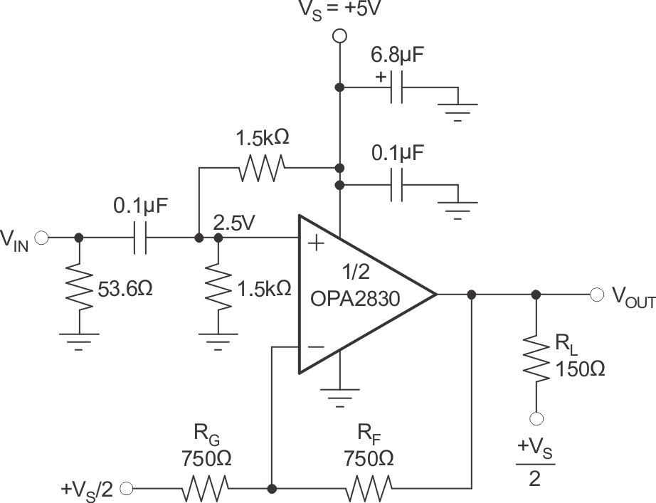
Figure 8-1 shows the ac-coupled, gain of +2 configuration used for the 5V Specifications and Typical Characteristics. For test purposes, the input impedance is set to 50Ω with a resistor to ground. Voltage swings reported in the Electrical Characteristics are taken directly at the input and output pins. For the circuit of Figure 8-1, the total effective load on the output at high frequencies is 150Ω || 1500Ω. The 1.5kΩ resistors at the noninverting input provide the common-mode bias voltage. The parallel combination equals the dc resistance at the inverting input (RF), reducing the dc output offset due to input bias current.
 Figure 8-1 AC-Coupled, G = +2, 5V
Single-Supply Specification and Test Circuit
Figure 8-1 AC-Coupled, G = +2, 5V
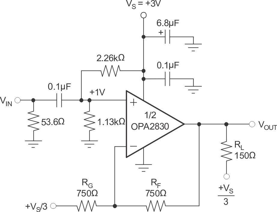
Single-Supply Specification and Test CircuitFigure 8-2 shows the ac-coupled, gain of +2 configuration used for the 3V Specifications and Typical Characteristics. Voltage swings reported in the Electrical Characteristics are taken directly at the input and output pins. For the circuit of Figure 8-2, the total effective load on the output at high frequencies is 150Ω || 1500Ω. The 1.13kΩ and 2.26kΩ resistors at the noninverting input provide the common-mode bias voltage. The parallel combination equals the dc resistance at the inverting input (RF), reducing the dc output offset due to input bias current.
 Figure 8-2 AC-Coupled, G = +2, 3V
Single-Supply Specification and Test Circuit
Figure 8-2 AC-Coupled, G = +2, 3V
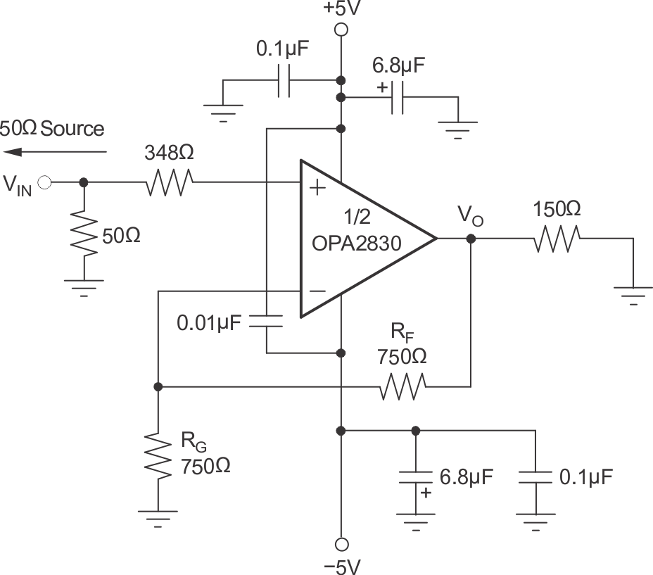
Single-Supply Specification and Test CircuitFigure 8-3 shows the dc-coupled, gain of +2, dual power-supply circuit configuration used as the basis of the ±5V Electrical Characteristics and Typical Characteristics. For test purposes, the input impedance is set to 50Ω with a resistor to ground and the output impedance is set to 150Ω with a series output resistor. Voltage swings reported in the specifications are taken directly at the input and output pins. For the circuit of Figure 8-3, the total effective load is 150Ω || 1.5kΩ. Two optional components are included in Figure 8-3. An additional resistor (348Ω) is included in series with the noninverting input. Combined with the 25Ω dc source resistance looking back towards the signal generator, this configuration gives an input bias current canceling resistance that matches the 375Ω source resistance seen at the inverting input (see the DC Accuracy and Offset Control section). In addition to the usual power-supply decoupling capacitors to ground, a 0.01μF capacitor is included between the two power-supply pins. In practical printed circuit board (PCB) layouts, this optional capacitor typically improves the 2nd-harmonic distortion performance by 3dB to 6dB.
 Figure 8-3 DC-Coupled, G = +2, Bipolar
Supply Specification and Test Circuit