SBOS309E August 2004 – December 2024 OPA2830
PRODUCTION DATA
- 1
- 1 Features
- 2 Applications
- 3 Description
- 4 Device Comparison Table
- 5 Pin Configurations and Functions
-
6 Specifications
- 6.1 Absolute Maximum Ratings
- 6.2 ESD Ratings
- 6.3 Recommended Operating Conditions
- 6.4 Thermal Information
- 6.5 Electrical Characteristics VS = ±5V
- 6.6 Electrical Characteristics VS = 5V
- 6.7 Electrical Characteristics VS = 3V
- 6.8 Typical Characteristics: VS = ±5V
- 6.9 Typical Characteristics: VS = ±5V, Differential Configuration
- 6.10 Typical Characteristics: VS = 5V
- 6.11 Typical Characteristics: VS = 5V, Differential Configuration
- 6.12 Typical Characteristics: VS = 3V
- 6.13 Typical Characteristics: VS = 3V, Differential Configuration
- 7 Parameter Measurement Information
-
8 Application and Implementation
- 8.1
Application Information
- 8.1.1 Wideband Voltage-Feedback Operation
- 8.1.2 Single-Supply ADC Interface
- 8.1.3 DC Level-Shifting
- 8.1.4 AC-Coupled Output Video Line Driver
- 8.1.5 Noninverting Amplifier With Reduced Peaking
- 8.1.6 Single-Supply Active Filter
- 8.1.7 Differential Low-Pass Active Filters
- 8.1.8 High-Pass Filters
- 8.1.9 High-Performance DAC Transimpedance Amplifier
- 8.1.10 Operating Suggestions Optimizing Resistor Values
- 8.1.11 Bandwidth vs Gain: Noninverting Operation
- 8.1.12 Inverting Amplifier Operation
- 8.1.13 Output Current and Voltages
- 8.1.14 Driving Capacitive Loads
- 8.1.15 Distortion Performance
- 8.1.16 Noise Performance
- 8.1.17 DC Accuracy and Offset Control
- 8.2 Power Supply Recommendations
- 8.3 Layout
- 8.1
Application Information
- 9 Device and Documentation Support
- 10Revision History
- 11Mechanical, Packaging, and Orderable Information
Package Options
Refer to the PDF data sheet for device specific package drawings
Mechanical Data (Package|Pins)
- D|8
- DGK|8
Thermal pad, mechanical data (Package|Pins)
Orderable Information
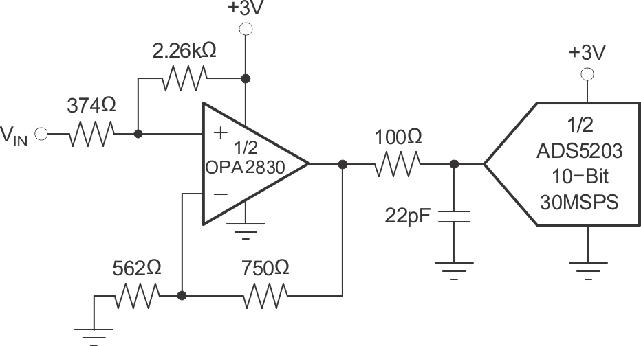
8.1.2 Single-Supply ADC Interface
The ADC interface of Figure 8-4 shows a dc-coupled, single-supply ADC driver circuit. Many systems are now requiring 3V to 5V supply capability of both the ADC and ADC driver. The OPA2830 provides excellent performance in this demanding application. The large input and output voltage ranges and low distortion support converters, such as the ADS5203 in the figure on page 1. The input level-shifting circuitry is designed so that VIN can be between 0V and 0.5V, while delivering an output voltage of 1V to 2V for the ADS5203.
 Figure 8-4 DC-Coupled, 3V ADC Driver