SBOS309E August 2004 – December 2024 OPA2830
PRODUCTION DATA
- 1
- 1 Features
- 2 Applications
- 3 Description
- 4 Device Comparison Table
- 5 Pin Configurations and Functions
-
6 Specifications
- 6.1 Absolute Maximum Ratings
- 6.2 ESD Ratings
- 6.3 Recommended Operating Conditions
- 6.4 Thermal Information
- 6.5 Electrical Characteristics VS = ±5V
- 6.6 Electrical Characteristics VS = 5V
- 6.7 Electrical Characteristics VS = 3V
- 6.8 Typical Characteristics: VS = ±5V
- 6.9 Typical Characteristics: VS = ±5V, Differential Configuration
- 6.10 Typical Characteristics: VS = 5V
- 6.11 Typical Characteristics: VS = 5V, Differential Configuration
- 6.12 Typical Characteristics: VS = 3V
- 6.13 Typical Characteristics: VS = 3V, Differential Configuration
- 7 Parameter Measurement Information
-
8 Application and Implementation
- 8.1
Application Information
- 8.1.1 Wideband Voltage-Feedback Operation
- 8.1.2 Single-Supply ADC Interface
- 8.1.3 DC Level-Shifting
- 8.1.4 AC-Coupled Output Video Line Driver
- 8.1.5 Noninverting Amplifier With Reduced Peaking
- 8.1.6 Single-Supply Active Filter
- 8.1.7 Differential Low-Pass Active Filters
- 8.1.8 High-Pass Filters
- 8.1.9 High-Performance DAC Transimpedance Amplifier
- 8.1.10 Operating Suggestions Optimizing Resistor Values
- 8.1.11 Bandwidth vs Gain: Noninverting Operation
- 8.1.12 Inverting Amplifier Operation
- 8.1.13 Output Current and Voltages
- 8.1.14 Driving Capacitive Loads
- 8.1.15 Distortion Performance
- 8.1.16 Noise Performance
- 8.1.17 DC Accuracy and Offset Control
- 8.2 Power Supply Recommendations
- 8.3 Layout
- 8.1
Application Information
- 9 Device and Documentation Support
- 10Revision History
- 11Mechanical, Packaging, and Orderable Information
Package Options
Refer to the PDF data sheet for device specific package drawings
Mechanical Data (Package|Pins)
- D|8
- DGK|8
Thermal pad, mechanical data (Package|Pins)
Orderable Information
8.1.3 DC Level-Shifting
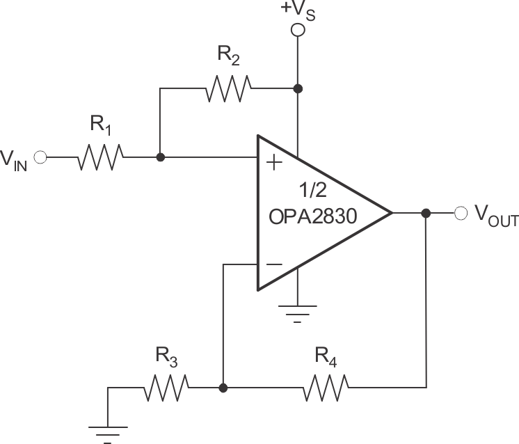
Figure 8-5 shows the general form of Figure 8-4 as a dc-coupled noninverting amplifier that level-shifts the input up to accommodate the desired output voltage range. Given the desired signal gain (G), and the amount VOUT must be shifted up (ΔVOUT) when VIN is at the center of the range, the following equations give the resistor values that produce the desired performance. Assume that R4 is between 200Ω and 1.5kΩ.
- NG = G + VOUT / VS
- R1 = R4 / G
- R2 = R4 / (NG – G)
- R3 = R4 / (NG – 1)
where:
- NG = 1 + R4 / R3
- VOUT = (G)VIN + (NG – G)VS
Ensure that VIN and VOUT stay within the specified input and output voltage ranges.
 Figure 8-5 DC Level
Shifting
Figure 8-5 DC Level
ShiftingThe circuit of Figure 8-4 is a good example of this type of application. The circuit designed to take VIN between 0V and 0.5V and produce VOUT between 1V and 2V when using a 3V supply. This means G = 2.00, and ΔVOUT = 1.50V – G × 0.25V = 1.00V. Plugging these values into the previous equations (with R4 = 750Ω) gives: NG = 2.33, R1 = 375Ω, R2 = 2.25kΩ, and R3 = 563Ω. The resistors were changed to the nearest standard values for the circuit of Figure 8-4.