SBOS309E August 2004 – December 2024 OPA2830
PRODUCTION DATA
- 1
- 1 Features
- 2 Applications
- 3 Description
- 4 Device Comparison Table
- 5 Pin Configurations and Functions
-
6 Specifications
- 6.1 Absolute Maximum Ratings
- 6.2 ESD Ratings
- 6.3 Recommended Operating Conditions
- 6.4 Thermal Information
- 6.5 Electrical Characteristics VS = ±5V
- 6.6 Electrical Characteristics VS = 5V
- 6.7 Electrical Characteristics VS = 3V
- 6.8 Typical Characteristics: VS = ±5V
- 6.9 Typical Characteristics: VS = ±5V, Differential Configuration
- 6.10 Typical Characteristics: VS = 5V
- 6.11 Typical Characteristics: VS = 5V, Differential Configuration
- 6.12 Typical Characteristics: VS = 3V
- 6.13 Typical Characteristics: VS = 3V, Differential Configuration
- 7 Parameter Measurement Information
-
8 Application and Implementation
- 8.1
Application Information
- 8.1.1 Wideband Voltage-Feedback Operation
- 8.1.2 Single-Supply ADC Interface
- 8.1.3 DC Level-Shifting
- 8.1.4 AC-Coupled Output Video Line Driver
- 8.1.5 Noninverting Amplifier With Reduced Peaking
- 8.1.6 Single-Supply Active Filter
- 8.1.7 Differential Low-Pass Active Filters
- 8.1.8 High-Pass Filters
- 8.1.9 High-Performance DAC Transimpedance Amplifier
- 8.1.10 Operating Suggestions Optimizing Resistor Values
- 8.1.11 Bandwidth vs Gain: Noninverting Operation
- 8.1.12 Inverting Amplifier Operation
- 8.1.13 Output Current and Voltages
- 8.1.14 Driving Capacitive Loads
- 8.1.15 Distortion Performance
- 8.1.16 Noise Performance
- 8.1.17 DC Accuracy and Offset Control
- 8.2 Power Supply Recommendations
- 8.3 Layout
- 8.1
Application Information
- 9 Device and Documentation Support
- 10Revision History
- 11Mechanical, Packaging, and Orderable Information
Package Options
Refer to the PDF data sheet for device specific package drawings
Mechanical Data (Package|Pins)
- D|8
- DGK|8
Thermal pad, mechanical data (Package|Pins)
Orderable Information
8.3.1.1 Input and ESD Protection
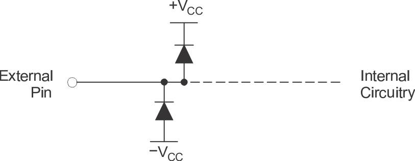
The OPA2830 is built using a very high-speed complementary bipolar process. The internal junction breakdown voltages are relatively low for these very small geometry devices. These breakdowns are reflected in the Absolute Maximum Ratings table. All device pins are protected with internal ESD protection diodes to the power supplies, as shown in Figure 8-17.
 Figure 8-17 Internal
ESD Protection
Figure 8-17 Internal
ESD ProtectionThese diodes provide moderate protection to input overdrive voltages greater than the supplies as well. The protection diodes can typically support 30mA continuous current. Where higher currents are possible (that is, in systems with ±15V supply parts driving into the OPA2830), current-limiting series resistors added into the two inputs. Keep these resistor values as low as possible because high values degrade both noise performance and frequency response.