SBOS309E August 2004 – December 2024 OPA2830
PRODUCTION DATA
- 1
- 1 Features
- 2 Applications
- 3 Description
- 4 Device Comparison Table
- 5 Pin Configurations and Functions
-
6 Specifications
- 6.1 Absolute Maximum Ratings
- 6.2 ESD Ratings
- 6.3 Recommended Operating Conditions
- 6.4 Thermal Information
- 6.5 Electrical Characteristics VS = ±5V
- 6.6 Electrical Characteristics VS = 5V
- 6.7 Electrical Characteristics VS = 3V
- 6.8 Typical Characteristics: VS = ±5V
- 6.9 Typical Characteristics: VS = ±5V, Differential Configuration
- 6.10 Typical Characteristics: VS = 5V
- 6.11 Typical Characteristics: VS = 5V, Differential Configuration
- 6.12 Typical Characteristics: VS = 3V
- 6.13 Typical Characteristics: VS = 3V, Differential Configuration
- 7 Parameter Measurement Information
-
8 Application and Implementation
- 8.1
Application Information
- 8.1.1 Wideband Voltage-Feedback Operation
- 8.1.2 Single-Supply ADC Interface
- 8.1.3 DC Level-Shifting
- 8.1.4 AC-Coupled Output Video Line Driver
- 8.1.5 Noninverting Amplifier With Reduced Peaking
- 8.1.6 Single-Supply Active Filter
- 8.1.7 Differential Low-Pass Active Filters
- 8.1.8 High-Pass Filters
- 8.1.9 High-Performance DAC Transimpedance Amplifier
- 8.1.10 Operating Suggestions Optimizing Resistor Values
- 8.1.11 Bandwidth vs Gain: Noninverting Operation
- 8.1.12 Inverting Amplifier Operation
- 8.1.13 Output Current and Voltages
- 8.1.14 Driving Capacitive Loads
- 8.1.15 Distortion Performance
- 8.1.16 Noise Performance
- 8.1.17 DC Accuracy and Offset Control
- 8.2 Power Supply Recommendations
- 8.3 Layout
- 8.1
Application Information
- 9 Device and Documentation Support
- 10Revision History
- 11Mechanical, Packaging, and Orderable Information
Package Options
Refer to the PDF data sheet for device specific package drawings
Mechanical Data (Package|Pins)
- D|8
- DGK|8
Thermal pad, mechanical data (Package|Pins)
Orderable Information
8.1.5 Noninverting Amplifier With Reduced Peaking
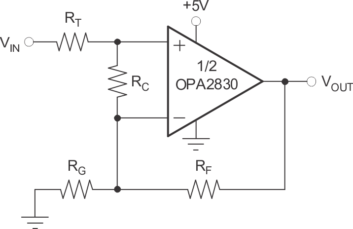
Figure 8-8 shows a noninverting amplifier that reduces peaking at low gains. The resistor RC compensates the OPA2830 to have higher Noise Gain (NG), which reduces the ac response peaking (typically 4dB at G = +1 without RC) without changing the dc gain. VIN needs to be a low impedance source, such as an op amp.
 Figure 8-8 Compensated Noninverting
Amplifier
Figure 8-8 Compensated Noninverting
AmplifierThe Noise Gain can be calculated as follows:


A unity-gain buffer can be designed by selecting RT = RF = 20.0Ω and RC = 40.2Ω (do not use RG). This gives a noise gain of 2, so the response is similar to the Characteristics Plots with G = +2 giving less peaking.