SBOS309E August 2004 – December 2024 OPA2830
PRODUCTION DATA
- 1
- 1 Features
- 2 Applications
- 3 Description
- 4 Device Comparison Table
- 5 Pin Configurations and Functions
-
6 Specifications
- 6.1 Absolute Maximum Ratings
- 6.2 ESD Ratings
- 6.3 Recommended Operating Conditions
- 6.4 Thermal Information
- 6.5 Electrical Characteristics VS = ±5V
- 6.6 Electrical Characteristics VS = 5V
- 6.7 Electrical Characteristics VS = 3V
- 6.8 Typical Characteristics: VS = ±5V
- 6.9 Typical Characteristics: VS = ±5V, Differential Configuration
- 6.10 Typical Characteristics: VS = 5V
- 6.11 Typical Characteristics: VS = 5V, Differential Configuration
- 6.12 Typical Characteristics: VS = 3V
- 6.13 Typical Characteristics: VS = 3V, Differential Configuration
- 7 Parameter Measurement Information
-
8 Application and Implementation
- 8.1
Application Information
- 8.1.1 Wideband Voltage-Feedback Operation
- 8.1.2 Single-Supply ADC Interface
- 8.1.3 DC Level-Shifting
- 8.1.4 AC-Coupled Output Video Line Driver
- 8.1.5 Noninverting Amplifier With Reduced Peaking
- 8.1.6 Single-Supply Active Filter
- 8.1.7 Differential Low-Pass Active Filters
- 8.1.8 High-Pass Filters
- 8.1.9 High-Performance DAC Transimpedance Amplifier
- 8.1.10 Operating Suggestions Optimizing Resistor Values
- 8.1.11 Bandwidth vs Gain: Noninverting Operation
- 8.1.12 Inverting Amplifier Operation
- 8.1.13 Output Current and Voltages
- 8.1.14 Driving Capacitive Loads
- 8.1.15 Distortion Performance
- 8.1.16 Noise Performance
- 8.1.17 DC Accuracy and Offset Control
- 8.2 Power Supply Recommendations
- 8.3 Layout
- 8.1
Application Information
- 9 Device and Documentation Support
- 10Revision History
- 11Mechanical, Packaging, and Orderable Information
Package Options
Refer to the PDF data sheet for device specific package drawings
Mechanical Data (Package|Pins)
- D|8
- DGK|8
Thermal pad, mechanical data (Package|Pins)
Orderable Information
3 Description
The OPA2830 is a dual, low-power, single-supply, wide-band, voltage-feedback amplifier designed to operate on a single 3V or 5V supply. The device also supports operation on ±5V or +10V supplies. The input range extends below the negative supply and to within 1.8V of the positive supply. Using complementary common-emitter outputs provides an output swing to within 25mV of either supply while driving 150Ω. High output drive current (±75mA) and low differential gain and phase errors also make this device an excellent choice for single-supply consumer video products.
Low distortion operation is provided by the high gain bandwidth product (100MHz) and slew rate (500V/μs), making the OPA2830 an excellent input buffer stage to 3V and 5V CMOS ADCs. Unlike other low-power, single-supply amplifiers, distortion performance improves as the signal swing decreases. A low 9.2nV/√Hz input voltage noise supports wide dynamic range operation.
The OPA2830 is available in an industry-standard SO-8 package. The OPA2830 is also available in a small VSSOP-8 package. For fixed-gain and line driver applications, consider the OPA2832.
| PART NUMBER(1) | PACKAGE(2) | PACKAGE SIZE(3) |
|---|---|---|
| OPA2830 | D (SOIC, 8) | 4.9mm × 6mm |
| DGK (VSSOP, 8) | 3mm × 3mm |
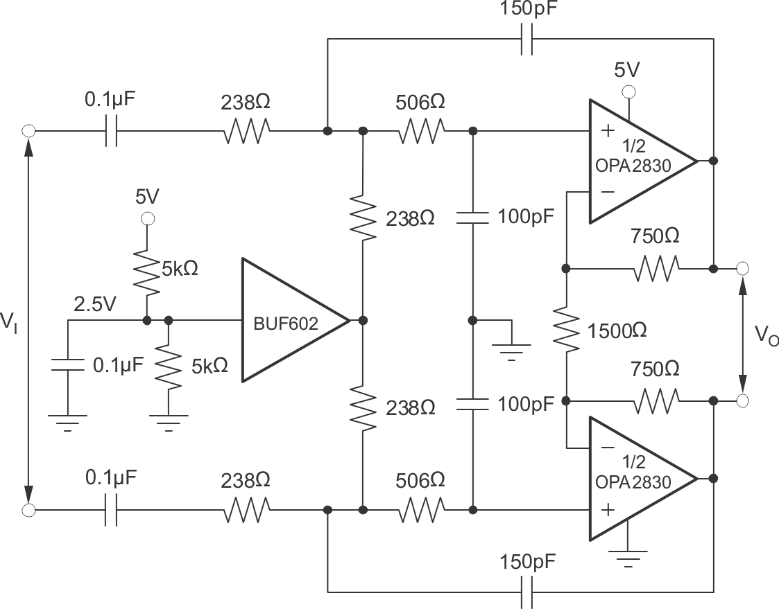
 DC-Coupled, 3V ADC Driver