SLOS713J January 2011 – March 2021 OPA2835 , OPA835
PRODUCTION DATA
- 1 Features
- 2 Applications
- 3 Description
- 4 Revision History
- 5 Device Comparision Table
- 6 Pin Configuration and Functions
-
7 Specifications
- 7.1 Absolute Maximum Ratings
- 7.2 ESD Ratings
- 7.3 Recommended Operating Conditions
- 7.4 Thermal Information: OPA835
- 7.5 Thermal Information: OPA2835
- 7.6 Electrical Characteristics: VS = 2.7 V
- 7.7 Electrical Characteristics: VS = 5 V
- 7.8 Typical Characteristics: VS = 2.7 V
- 7.9 Typical Characteristics: VS = 5 V
- 8 Detailed Description
-
9 Application and Implementation
- 9.1
Application Information
- 9.1.1 Noninverting Amplifier
- 9.1.2 Inverting Amplifier
- 9.1.3 Instrumentation Amplifier
- 9.1.4 Attenuators
- 9.1.5 Single-Ended to Differential Amplifier
- 9.1.6 Differential to Single-Ended Amplifier
- 9.1.7 Differential-to-Differential Amplifier
- 9.1.8 Gain Setting With OPA835 RUN Integrated Resistors
- 9.1.9 Pulse Application With Single-Supply
- 9.1.10 ADC Driver Performance
- 9.2 Typical Application
- 9.1
Application Information
- 10Power Supply Recommendations
- 11Layout
- 12Device and Documentation Support
- 13Mechanical, Packaging, and Orderable Information
Package Options
Mechanical Data (Package|Pins)
Thermal pad, mechanical data (Package|Pins)
Orderable Information
8.4.1 Split-Supply Operation (±1.25 V to ±2.75 V)
To facilitate testing with common lab equipment, the OPA835 EVM ( see OPA835DBV and OPA836DBV EVM User's Guide (SLOU314) ) is built to allow split-supply operation. This configuration eases lab testing because the mid-point between the power rails is ground, and most signal generators, network analyzers, oscilloscopes, spectrum analyzers and other lab equipment have inputs and outputs with a ground reference.
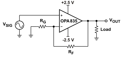
Figure 8-6 shows a simple noninverting configuration analogous to Figure 8-1 with ±2.5-V supply and VREF equal to ground. The input and output will swing symmetrically around ground. For ease of use, split supplies are preferred in systems where signals swing around ground.
 Figure 8-6 Split-Supply Operation