SBOS673D September 2017 – December 2018 OPA2837 , OPA837
PRODUCTION DATA.
- 1 Features
- 2 Applications
- 3 Description
- 4 Revision History
- 5 Pin Configuration and Functions
-
6 Specifications
- 6.1 Absolute Maximum Ratings
- 6.2 ESD Ratings
- 6.3 Recommended Operating Conditions
- 6.4 Thermal Information: OPA837
- 6.5 Thermal Information: OPA2837
- 6.6 Electrical Characteristics: VS = 5 V
- 6.7 Electrical Characteristics: VS = 3 V
- 6.8 Typical Characteristics: VS = 5.0 V
- 6.9 Typical Characteristics: VS = 3.0 V
- 6.10 Typical Characteristics: ±2.5-V to ±1.5-V Split Supply
- 7 Detailed Description
-
8 Application and Implementation
- 8.1
Application Information
- 8.1.1 Noninverting Amplifier
- 8.1.2 Inverting Amplifier
- 8.1.3 Output DC Error Calculations
- 8.1.4 Output Noise Calculations
- 8.1.5 Instrumentation Amplifier
- 8.1.6 Attenuators
- 8.1.7 Differential to Single-Ended Amplifier
- 8.1.8 Differential-to-Differential Amplifier
- 8.1.9 Pulse Application With Single-Supply Circuit
- 8.1.10 ADC Driver Performance
- 8.2 Typical Applications
- 8.1
Application Information
- 9 Power Supply Recommendations
- 10Layout
- 11Device and Documentation Support
- 12Mechanical, Packaging, and Orderable Information
Package Options
Mechanical Data (Package|Pins)
Thermal pad, mechanical data (Package|Pins)
- RUN|10
Orderable Information
7.4.2 Single-Supply Operation (2.7 V to 5.4 V)
Most newer systems use a single power supply to improve efficiency and to simplify power-supply design. The OPAx837 can be used with single-supply power (ground for the negative supply) with no change in performance from split supply, as long as the input and output pins are biased within the linear operating region of the device. The outputs nominally swing rail-to-rail with approximately a 100-mV headroom required for linear operation. The inputs can typically swing 0.2 V below the negative rail (typically ground) and to within 1.2 V of the positive supply. For DC-coupled single-supply operation, the input swing is below the available output swing range for noninverting gains greater than 1.30 V/V. Typically, the 1.2-V input headroom required to the positive supply only limits output swing range for a unity-gain buffer.
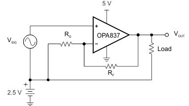
To change the circuit from split supply to single-supply, level shift all voltages by half the difference between the power-supply rails. For example, Figure 69 depicts changing from a ±2.5-V split supply to a 5-V single-supply. The load is shown as mid-supply referenced but can be grounded as well.
 Figure 69. Single-Supply Concept
 A practical circuit has an amplifier or other circuit providing the bias voltage for the input, and the output of this amplifier stage provides the bias for the next stage.
Figure 70 shows a typical noninverting amplifier circuit. With 5-V single-supply, a mid-supply reference generator is needed to bias the negative side through RG. To cancel the voltage offset that is otherwise caused by the input bias currents, R1 is selected to be equal to RF in parallel with RG. For example, if a gain of 2 V/V is required and RF = 2 kΩ, select RG = 2 kΩ to set the gain, and R1 = 1 kΩ for bias current cancellation which reduces the output DC error to IOS × RF. The value for C is dependent on the reference, and TI recommends a value of at least 0.1 µF to limit noise. The frequency response flatness is impacted by the AC impedance, including the reference and capacitor added to the RG element.
 Figure 70. Noninverting Single-Supply Operation With Reference
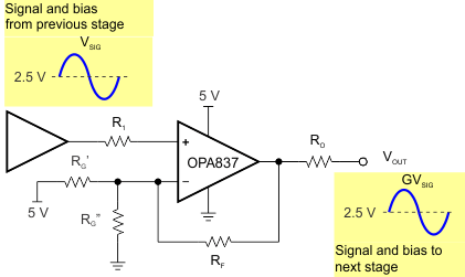
 Figure 71 shows a similar noninverting single-supply scenario with the reference generator replaced by the Thevenin equivalent using resistors and the positive supply. RG’ and RG” form a resistor divider from the 5-V supply and are used to bias the negative side with the parallel sum equal to the equivalent RG to set the gain. To cancel the voltage offset that is otherwise caused by the input bias currents, R1 is selected to be equal to RF in parallel with RG’ in parallel with RG” (R1= RF || RG’ || RG”). For example, if a gain of 2 V/V is required and RF = 2 kΩ, selecting RG’ = RG” = 4 kΩ gives an quivalent parallel sum of 2 kΩ, sets the gain to 2, and references the input to mid-supply (2.5 V). R1 is set to 1 kΩ for bias current cancellation. The resistor divider costs less than the 2.5-V reference in Figure 70 but increases the current from the 5-V supply. Any noise or variation on the 5-V supply now also comes into the circuit as an input through the biasing path.
 Figure 71. Noninverting Single-Supply Operation With Resistor Mid-Supply Biasing
 Figure 72 shows a typical inverting amplifier circuit. With a 5-V single supply, a mid-supply reference generator is needed to bias the positive side through R1. To cancel the voltage offset that is otherwise caused by the input bias currents, R1 is selected to be equal to RF in parallel with RG. For example, if a gain of –2 V/V is required and RF = 2 kΩ, select RG = 1 kΩ to set the gain and R1 = 667 Ω for bias current cancellation. The value for C is dependent on the reference, but TI recommends a value of at least 0.1 µF to limit noise into the op amp.
 Figure 72. Inverting Single-Supply Operation With Reference
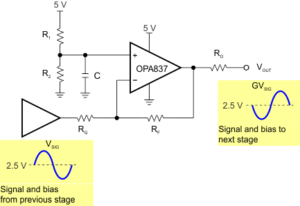
 Figure 73 shows a similar inverting single-supply scenario with the reference generator replaced by the Thevenin equivalent using resistors and the positive supply. R1 and R2 form a resistor divider from the 5-V supply and are used to bias the positive side. To cancel the voltage offset that is otherwise caused by the input bias currents, set the parallel value of R1 and R2 equal to the parallel value of RF and RG. C must be added to limit coupling of noise into the positive input. For example, if gain of –2 V/V is required and RF = 2 kΩ, select RG = 1 kΩ to set the gain. R1 = R2 = 2 × 667 Ω = 1.33 kΩ for the mid-supply voltage bias and for op-amp input-bias current cancellation. A good value for C is 0.1 µF. The resistor divider costs less than the 2.5-V reference in Figure 72 but increases the current from the 5-V supply. Any noise or variation in the 5-V supply also comes into the circuit through this bias setup but be band-limited by the pole formed with R1 || R2 and C.
 Figure 73. Inverting Single-Supply Operation With Resistor Midsupply Biasing
 These examples are only a few of the ways to implement a single-supply design. Many other designs exist that can often be simpler if AC-coupled inputs are allowed. A good compilation of options can be found in the Single-Supply Op Amp Design Techniques application report.