SBOSAG6 November 2023 OPA2994-Q1
ADVANCE INFORMATION
- 1
- 1 Features
- 2 Applications
- 3 Description
- 4 Pin Configuration and Functions
- 5 Specifications
- 6 Detailed Description
- 7 Application and Implementation
- 8 Device and Documentation Support
- 9 Revision History
- 10Mechanical, Packaging, and Orderable Information
Package Options
Refer to the PDF data sheet for device specific package drawings
Mechanical Data (Package|Pins)
- D|8
Thermal pad, mechanical data (Package|Pins)
Orderable Information
10.1 Tape and Reel Information
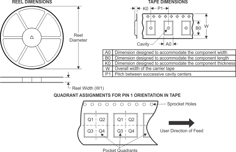
| Device | Package Type | Package Drawing | Pins | SPQ | Reel Diameter (mm) | Reel Width W1 (mm) | A0 (mm) | B0 (mm) | K0 (mm) | P1 (mm) | W (mm) | Pin1 Quadrant |
|---|---|---|---|---|---|---|---|---|---|---|---|---|
| OPA994QDBVRQ1 | SOT-23 | DBV | 5 | 3000 | 180.0 | 8.4 | 3.2 | 3.2 | 1.4 | 4.0 | 8.0 | Q3 |
| OPA2994QDRQ1 | SOIC | D | 8 | 3000 | 330.0 | 12.4 | 6.4 | 5.2 | 2.1 | 8.0 | 12.0 | Q1 |
| OPA2994QDGKRQ1 | VSSOP | DGK | 8 | 2500 | 330.0 | 12.4 | 5.3 | 3.4 | 1.4 | 8.0 | 12.0 | Q1 |
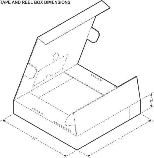
| Device | Package Type | Package Drawing | Pins | SPQ | Length (mm) | Width (mm) | Height (mm) |
|---|---|---|---|---|---|---|---|
| OPA994QDBVRQ1 | SOT-23 | DBV | 5 | 3000 | 210.0 | 185.0 | 35.0 |
| OPA2994QDRQ1 | SOIC | D | 8 | 3000 | 356.0 | 356.0 | 35.0 |
| OPA2994QDGKRQ1 | VSSOP | DGK | 8 | 2500 | 366.0 | 364.0 | 50.0 |