SBOSAI0B December 2023 – September 2024 OPA310-Q1
PRODMIX
- 1
- 1 Features
- 2 Applications
- 3 Description
- 4 Pin Configuration and Functions
- 5 Specifications
- 6 Detailed Description
- 7 Application and Implementation
- 8 Device and Documentation Support
- 9 Revision History
- 10Mechanical, Packaging, and Orderable Information
Package Options
Refer to the PDF data sheet for device specific package drawings
Mechanical Data (Package|Pins)
- DBV|5
- DBV|6
- DCK|5
- DCK|6
Thermal pad, mechanical data (Package|Pins)
Orderable Information
4 Pin Configuration and Functions
 Figure 4-1 OPA310-Q1 DBV Package
5-Pin SOT-23
(Top View)
 Figure 4-2 OPA310-Q1 DCK Package
5-Pin SC70
(Top View)
Table 4-1 Pin Functions: OPA310-Q1
| PIN | TYPE(1) | DESCRIPTION | ||
|---|---|---|---|---|
| NAME | SOT-23 | SC70 | ||
| IN– | 4 | 3 | I | Inverting input |
| IN+ | 3 | 1 | I | Noninverting input |
| OUT | 1 | 4 | O | Output |
| V– | 2 | 2 | I | Negative (low) supply or ground (for single-supply operation) |
| V+ | 5 | 5 | I | Positive (high) supply |
(1) I = input, O = output
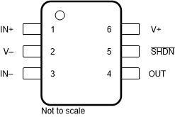
 Figure 4-3 OPA310S-Q1 DBV Package
6-Pin SOT-23
(Top View)
 Figure 4-4 OPA310S-Q1 DCK Package
6-Pin SC70
(Top View)
Table 4-2 Pin Functions: OPA310S-Q1
| PIN | TYPE(1) | DESCRIPTION | ||
|---|---|---|---|---|
| NAME | SOT-23 | SC70 | ||
| IN– | 4 | 3 | I | Inverting input |
| IN+ | 3 | 1 | I | Noninverting input |
| OUT | 1 | 4 | O | Output |
| SHDN | 5 | 5 | I | Shutdown: low =
amp disabled, high = amp enabled See Shutdown Function for more information |
| V– | 2 | 2 | I | Negative (low) supply or ground (for single-supply operation) |
| V+ | 6 | 6 | I | Positive (high) supply |
(1) I = input, O = output
 Figure 4-5 OPA2310-Q1 D and DGK Package
8-Pin SOIC and VSSOP
(Top View)
Table 4-3 Pin Functions: OPA2310-Q1
| PIN | TYPE(1) | DESCRIPTION | ||
|---|---|---|---|---|
| NAME | NO. | |||
| IN1– | 2 | I | Inverting input, channel 1 | |
| IN1+ | 3 | I | Noninverting input, channel 1 | |
| IN2– | 6 | I | Inverting input, channel 2 | |
| IN2+ | 5 | I | Noninverting input, channel 2 | |
| OUT1 | 1 | O | Output, channel 1 | |
| OUT2 | 7 | O | Output, channel 2 | |
| V– | 4 | I | Negative (low) supply or ground (for single-supply operation) | |
| V+ | 8 | I | Positive (high) supply | |
(1) I = input, O = output
 Figure 4-6 OPA4310-Q1 D and PW Package
14-Pin SOIC and TSSOP
(Top View)
Table 4-4 Pin Functions: OPA4310-Q1
| PIN | TYPE(1) | DESCRIPTION | |
|---|---|---|---|
| NAME | NO. | ||
| IN1– | 2 | I | Inverting input, channel 1 |
| IN1+ | 3 | I | Noninverting input, channel 1 |
| IN2– | 6 | I | Inverting input, channel 2 |
| IN2+ | 5 | I | Noninverting input, channel 2 |
| IN3– | 9 | I | Inverting input, channel 3 |
| IN3+ | 10 | I | Noninverting input, channel 3 |
| IN4– | 13 | I | Inverting input, channel 4 |
| IN4+ | 12 | I | Noninverting input, channel 4 |
| OUT1 | 1 | O | Output, channel 1 |
| OUT2 | 7 | O | Output, channel 2 |
| OUT3 | 8 | O | Output, channel 3 |
| OUT4 | 14 | O | Output, channel 4 |
| V– | 11 | I | Negative (low) supply or ground (for single-supply operation) |
| V+ | 4 | I | Positive (high) supply |
(1) I = input, O = output