SBOSAI0B December 2023 – September 2024 OPA310-Q1
PRODMIX
- 1
- 1 Features
- 2 Applications
- 3 Description
- 4 Pin Configuration and Functions
- 5 Specifications
- 6 Detailed Description
- 7 Application and Implementation
- 8 Device and Documentation Support
- 9 Revision History
- 10Mechanical, Packaging, and Orderable Information
Package Options
Refer to the PDF data sheet for device specific package drawings
Mechanical Data (Package|Pins)
- DBV|5
- DBV|6
- DCK|5
- DCK|6
Thermal pad, mechanical data (Package|Pins)
Orderable Information
6.3.6 EMI Rejection
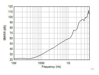
The OPAx310-Q1 uses integrated electromagnetic interference (EMI) filtering to reduce the effects of EMI from sources such as wireless communications (radio frequency interference - RFI) and densely-populated boards with a mix of analog signal chain and digital components. EMI immunity can be improved with circuit design techniques; the OPAx310-Q1 benefits from these design improvements. Texas Instruments has developed the ability to accurately measure and quantify the immunity of an operational amplifier over a broad frequency spectrum extending from 10MHz to 6GHz. Figure 6-4 shows the results of this testing on the OPAx310-Q1. Table 6-1 shows the EMIRR IN+ values for the OPAx310-Q1 at particular frequencies commonly encountered in real-world applications. The EMI Rejection Ratio of Operational Amplifiers application report contains detailed information on the topic of EMIRR performance relating to op amps and is available for download from www.ti.com.
 Figure 6-4 EMIRR Testing
| FREQUENCY | APPLICATION OR ALLOCATION | EMIRR IN+ |
|---|---|---|
| 400MHz | Mobile radio, mobile satellite, space operation, weather, radar, ultra-high frequency (UHF) applications | 48dB |
| 900MHz | Global system for mobile communications (GSM) applications, radio communication, navigation, GPS (to 1.6GHz), GSM, aeronautical mobile, UHF applications | 58dB |
| 1.8GHz | GSM applications, mobile personal communications, broadband, satellite, L-band (1GHz to 2GHz) | 75dB |
| 2.4GHz | 802.11b, 802.11g, 802.11n, Bluetooth®, mobile personal communications, industrial, scientific and medical (ISM) radio band, amateur radio and satellite, S-band (2GHz to 4GHz) | 90dB |
| 3.6GHz | Radiolocation, aero communication and navigation, satellite, mobile, S-band | 95dB |
| 5GHz | 802.11a, 802.11n, aero communication and navigation, mobile communication, space and satellite operation, C-band (4GHz to 8GHz) | 102dB |