SBOSAI0B December 2023 – September 2024 OPA310-Q1
PRODMIX
- 1
- 1 Features
- 2 Applications
- 3 Description
- 4 Pin Configuration and Functions
- 5 Specifications
- 6 Detailed Description
- 7 Application and Implementation
- 8 Device and Documentation Support
- 9 Revision History
- 10Mechanical, Packaging, and Orderable Information
Package Options
Refer to the PDF data sheet for device specific package drawings
Mechanical Data (Package|Pins)
- DBV|5
- DBV|6
- DCK|5
- DCK|6
Thermal pad, mechanical data (Package|Pins)
Orderable Information
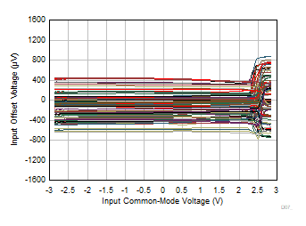
6.3.2 Rail-to-Rail Input
The input common-mode voltage range of the OPAx310-Q1 series extends to either supply rails. This is true even when operating at the ultra-low supply voltage of 1.5V, all the way up to the standard supply voltage of 5.5V. This performance is achieved with a complementary input stage: an N-channel input differential pair in parallel with a P-channel differential pair. Refer to the Functional Block Diagram for more details.
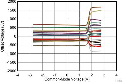
For most amplifiers with a complementary input stage, one of the input pairs, usually the P-channel input pair, is designed to deliver slightly better performance in terms of input offset voltage, offset drift over the N-channel pair. Consequently, the P-channel pair is designed to cover the majority of the common mode range with the N-channel pair slated to slowly take over at a certain threshold voltage from the positive rail. Just after the threshold voltage, both the input pairs are in operation for a small range referred to as the transition region. Beyond this region, the N-channel pair completely takes over. Within the transition region, PSRR, CMRR, offset voltage, offset drift, and THD can be degraded compared to device operation outside this region. Hence, most applications generally prefer operating in the P-channel input range where the performance is slightly better.
For the OPAx310-Q1, the P-channel pair is typically active for input voltages from (V–) to (V+) – 0.4V and the N-channel pair is typically active for input voltages from the positive supply to (V+) – 0.4V. The transition region occurs typically from (V+) – 0.5V to (V+) – 0.3V, in which both pairs are on. These voltage levels mentioned above can vary with process variations associated with threshold voltage of transistors. In the OPAx310-Q1, 200mV transition region mentioned above can vary up to 200mV in either direction. Thus, the transition region (both stages on) can range from (V+) – 0.7V to (V+) – 0.5V on the low end, up to (V+) – 0.3V to (V+) – 0.1V on the high end.
Recollecting the fact that a P-channel input pair usually offers better performance over a N-channel input pair, the OPAx310-Q1 is designed to offer a much wider P-channel input pair range, in comparison to most complimentary input amplifiers in the industry. A side-by-side comparison of the OPAx310-Q1 and the TLV900x is provided below. Note that the TLV900x is designed for P-channel pair operation only until 1.4V from the positive rail, while the OPAx310-Q1 is designed for P-channel pair operation until 0.7V from the positive rail. This additional 700mV of P-channel input pair range for the OPAx310-Q1 is particularly useful when operating at lower supply voltages (1.5V, 1.8V, and so forth) where the P-channel input range usually gets limited to a great extent.
Thus the wide common mode swing of input signal can be accommodated more easily within the P-channel input pair of the OPAx310-Q1, while likely avoiding the transition region, thereby maintaining linearity.

| V+ = 2.75V, V– = –2.75V |

| V+ = 2.75V, V– = –2.75V |