SBOS841A November 2016 – January 2017 OPA2316-Q1 , OPA316-Q1 , OPA4316-Q1
PRODUCTION DATA.
- 1 Features
- 2 Applications
- 3 Description
- 4 Revision History
- 5 Pin Configuration and Functions
- 6 Specifications
- 7 Detailed Description
- 8 Application and Implementation
- 9 Power Supply Recommendations
- 10Layout
- 11Device and Documentation Support
- 12Mechanical, Packaging, and Orderable Information
Package Options
Mechanical Data (Package|Pins)
- DBV|5
Thermal pad, mechanical data (Package|Pins)
Orderable Information
6 Specifications
6.1 Absolute Maximum Ratings
over operating free-air temperature (unless otherwise noted)(1)| MIN | MAX | UNIT | |||
|---|---|---|---|---|---|
| Supply voltage | 7 | V | |||
| Signal input pins | Voltage(2) | Common-mode | (V–) – 0.5 | (V+) + 0.5 | V |
| Differential | (V+) – (V–) + 0.2 | V | |||
| Current(2) | –10 | 10 | mA | ||
| Output short-circuit(3) | Continuous | ||||
| TA | Operating temperature | –55 | 150 | °C | |
| TJ | Junction temperature | 150 | °C | ||
| Tstg | Storage temperature | –65 | 150 | °C | |
(1) Stresses beyond those listed under Absolute Maximum Ratings may cause permanent damage to the device. These are stress ratings only, which do not imply functional operation of the device at these or any other conditions beyond those indicated under Recommended Operating Conditions. Exposure to absolute-maximum-rated conditions for extended periods may affect device reliability.
(2) Input pins are diode-clamped to the power-supply rails. Current limit input signals that can swing more than 0.5 V beyond the supply rails to 10 mA or less.
(3) Short-circuit to ground, one amplifier per package.
6.2 ESD Ratings
| VALUE | UNIT | |||
|---|---|---|---|---|
| V(ESD) | Electrostatic discharge | Human-body model (HBM), per AEC Q100-002(1) | ±4000 | V |
| Charged-device model (CDM), per AEC Q100-011 | ±750 | |||
(1) AEC Q100-002 indicates that HBM stressing shall be in accordance with the ANSI/ESDA/JEDEC JS-001 specification.
6.3 Recommended Operating Conditions
over operating free-air temperature range (unless otherwise noted)| MIN | MAX | UNIT | |||
|---|---|---|---|---|---|
| VS | Supply voltage | 1.8 | 5.5 | V | |
| Specified temperature | –40 | 125 | °C | ||
6.4 Thermal Information: OPA316-Q1
| THERMAL METRIC(1) | OPA316-Q1 | UNIT | |
|---|---|---|---|
| DBV (SOT-23) | |||
| 5 PINS | |||
| RθJA | Junction-to-ambient thermal resistance(2) | 221.7 | °C/W |
| RθJC(top) | Junction-to-case(top) thermal resistance(3) | 144.7 | °C/W |
| RθJB | Junction-to-board thermal resistance(4) | 49.7 | °C/W |
| ψJT | Junction-to-top characterization parameter(5) | 26.1 | °C/W |
| ψJB | Junction-to-board characterization parameter(6) | 49 | °C/W |
| RθJC(bot) | Junction-to-case(bottom) thermal resistance(7) | N/A | °C/W |
(1) For more information about traditional and new thermal metrics, see the Semiconductor and IC Package Thermal Metrics application report.
(2) The junction-to-ambient thermal resistance under natural convection is obtained in a simulation on a JEDEC-standard, high-K board, as specified in JESD51-7, in an environment described in JESD51-2a.
(3) The junction-to-case (top) thermal resistance is obtained by simulating a cold plate test on the package top. No specific JEDEC-standard test exists, but a close description can be found in the ANSI SEMI standard G30-88.
(4) The junction-to-board thermal resistance is obtained by simulating in an environment with a ring cold plate fixture to control the PCB temperature, as described in JESD51-8.
(5) The junction-to-top characterization parameter, ψJT, estimates the junction temperature of a device in a real system and is extracted from the simulation data for obtaining RθJA, using a procedure described in JESD51-2a (sections 6 and 7).
(6) The junction-to-board characterization parameter, ψJB, estimates the junction temperature of a device in a real system and is extracted from the simulation data for obtaining RθJA, using a procedure described in JESD51-2a (sections 6 and 7).
(7) The junction-to-case (bottom) thermal resistance is obtained by simulating a cold plate test on the exposed (power) pad. No specific JEDEC standard test exists, but a close description can be found in the ANSI SEMI standard G30-88.
6.5 Thermal Information: OPA2316-Q1
| THERMAL METRIC(1) | OPA2316-Q1 | UNIT | |
|---|---|---|---|
| DGK (VSSOP) | |||
| 8 PINS | |||
| RθJA | Junction-to-ambient thermal resistance(2) | 186.6 | °C/W |
| RθJC(top) | Junction-to-case(top) thermal resistance(3) | 78.8 | °C/W |
| RθJB | Junction-to-board thermal resistance(4) | 107.9 | °C/W |
| ψJT | Junction-to-top characterization parameter(5) | 15.5 | °C/W |
| ψJB | Junction-to-board characterization parameter(6) | 106.3 | °C/W |
| RθJC(bot) | Junction-to-case(bottom) thermal resistance(7) | N/A | °C/W |
(1) For more information about traditional and new thermal metrics, see the Semiconductor and IC Package Thermal Metrics application report.
(2) The junction-to-ambient thermal resistance under natural convection is obtained in a simulation on a JEDEC-standard, high-K board, as specified in JESD51-7, in an environment described in JESD51-2a.
(3) The junction-to-case (top) thermal resistance is obtained by simulating a cold plate test on the package top. No specific JEDEC-standard test exists, but a close description can be found in the ANSI SEMI standard G30-88.
(4) The junction-to-board thermal resistance is obtained by simulating in an environment with a ring cold plate fixture to control the PCB temperature, as described in JESD51-8.
(5) The junction-to-top characterization parameter, ψJT, estimates the junction temperature of a device in a real system and is extracted from the simulation data for obtaining RθJA, using a procedure described in JESD51-2a (sections 6 and 7).
(6) The junction-to-board characterization parameter, ψJB, estimates the junction temperature of a device in a real system and is extracted from the simulation data for obtaining RθJA, using a procedure described in JESD51-2a (sections 6 and 7).
(7) The junction-to-case (bottom) thermal resistance is obtained by simulating a cold plate test on the exposed (power) pad. No specific JEDEC standard test exists, but a close description can be found in the ANSI SEMI standard G30-88.
6.6 Thermal Information: OPA4316-Q1
| THERMAL METRIC(1) | OPA4316-Q1 | UNIT | |
|---|---|---|---|
| PW (TSSOP) | |||
| 14 PINS | |||
| RθJA | Junction-to-ambient thermal resistance(2) | 117.2 | °C/W |
| RθJC(top) | Junction-to-case(top) thermal resistance(3) | 46.2 | °C/W |
| RθJB | Junction-to-board thermal resistance(4) | 58.9 | °C/W |
| ψJT | Junction-to-top characterization parameter(5) | 4.9 | °C/W |
| ψJB | Junction-to-board characterization parameter(6) | 58.3 | °C/W |
| RθJC(bot) | Junction-to-case(bottom) thermal resistance(2) | N/A | °C/W |
(1) For more information about traditional and new thermal metrics, see the Semiconductor and IC Package Thermal Metrics application report.
(2) The junction-to-case (bottom) thermal resistance is obtained by simulating a cold plate test on the exposed (power) pad. No specific JEDEC standard test exists, but a close description can be found in the ANSI SEMI standard G30-88.
6.7 Electrical Characteristics
VS (total supply voltage) = (V+) – (V–) = 1.8 V to 5.5 V.at TA = 25°C, RL = 10 kΩ connected to VS / 2, VCM = VS / 2, and VOUT = VS / 2, unless otherwise noted
| PARAMETER | TEST CONDITIONS | MIN | TYP | MAX | UNIT | ||
|---|---|---|---|---|---|---|---|
| OFFSET VOLTAGE | |||||||
| VOS | Input offset voltage | VS = 5 V | ±0.5 | ±2.5 | mV | ||
| VS = 5 V, TA = –40°C to 125°C | ±3.5 | mV | |||||
| dVOS/dT | Drift | VS = 5 V, TA = –40°C to 125°C | ±2 | ±10 | μV/°C | ||
| PSRR | vs power supply | VS = 1.8 V – 5.5 V, VCM = (V–) | ±30 | ±150 | µV/V | ||
| VS = 1.8 V – 5.5 V, VCM = (V–), TA = –40°C to 125°C | ±250 | µV/V | |||||
| Channel separation, dc | At dc | 10 | µV/V | ||||
| INPUT VOLTAGE RANGE | |||||||
| VCM | Common-mode voltage | VS = 1.8 V to 2.5 V | (V–) – 0.2 | (V+) | V | ||
| VS = 2.5 V to 5.5 V | (V–) – 0.2 | (V+) + 0.2 | V | ||||
| CMRR | Common-mode rejection ratio | VS = 1.8 V, (V–) – 0.2 V < VCM < (V+) – 1.4 V, TA= –40°C to 125°C |
70 | 86 | dB | ||
| VS = 5.5 V, (V–) – 0.2 V < VCM < (V+) – 1.4 V, TA= –40°C to 125°C |
76 | 90 | dB | ||||
| VS = 1.8 V, VCM = –0.2 V to 1.8 V, TA= –40°C to 125°C |
57 | 72 | dB | ||||
| VS = 5.5 V, VCM = –0.2 V to 5.7 V, TA= –40°C to 125°C |
65 | 80 | dB | ||||
| INPUT BIAS CURRENT | |||||||
| IB | Input bias current | ±5 | ±15 | pA | |||
| TA= –40°C to 125°C | ±15 | nA | |||||
| IOS | Input offset current | ±2 | ±15 | pA | |||
| TA= –40°C to 125°C | ±8 | nA | |||||
| NOISE | |||||||
| En | Input voltage noise (peak-to-peak) | VS = 5 V, f = 0.1 Hz to 10 Hz | 3 | μVPP | |||
| en | Input voltage noise density | VS = 5 V, f = 1 kHz | 11 | nV/√Hz | |||
| in | Input current noise density | f = 1 kHz | 1.3 | fA/√Hz | |||
| INPUT IMPEDANCE | |||||||
| ZID | Differential | 2 || 2 | 1016Ω || pF | ||||
| ZIC | Common-mode | 2 || 4 | 1011Ω || pF | ||||
| OPEN-LOOP GAIN | |||||||
| AOL | Open-loop voltage gain | VS = 1.8 V, (V–) + 0.04 V < VO < (V+) – 0.04 V, RL = 10 kΩ |
94 | 100 | dB | ||
| VS = 5.5 V, (V–) + 0.05 V < VO < (V+) – 0.05 V, RL = 10 kΩ |
104 | 110 | dB | ||||
| VS = 1.8 V, (V–) + 0.1 V < VO < (V+) – 0.1 V, RL = 2 kΩ |
90 | 96 | dB | ||||
| VS = 5.5 V, (V–) + 0.15 V < VO < (V+) – 0.15 V, RL = 2 kΩ |
100 | 106 | dB | ||||
| VS = 5.5 V, (V–) + 0.05 V < VO < (V+) – 0.05 V, RL = 10 kΩ, TA= –40°C to 125°C |
86 | dB | |||||
| VS = 5.5 V, (V–) + 0.15 V < VO < (V+) – 0.15 V, RL = 2 kΩ, TA= –40°C to 125°C |
84 | dB | |||||
| FREQUENCY RESPONSE | |||||||
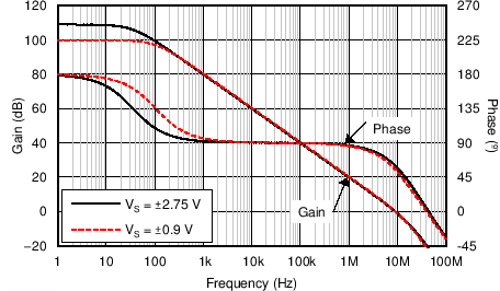
| GBP | Gain bandwidth product | VS = 5 V, G = 1 | 10 | MHz | |||
| φm | Phase margin | VS = 5 V, G = 1 | 60 | Degrees | |||
| SR | Slew rate | VS = 5 V, G = 1 | 6 | V/μs | |||
| tS | Settling time | To 0.1%, VS = 5 V, 2-V step , G = 1, CL = 100 pF | 1 | μs | |||
| To 0.01%, VS = 5 V, 2-V step , G = 1, CL = 100 pF | 1.66 | μs | |||||
| tOR | Overload recovery time | VS = 5 V, VIN × gain = VS | 0.3 | μs | |||
| THD + N | Total harmonic distortion + noise(1) | VS = 5 V, VO = 0.5 VRMS, G = 1 f = 1 kHz |
0.0008% | ||||
| OUTPUT | |||||||
| VO | Voltage output swing from supply rails | VS = 1.8 V, RL = 10 kΩ, TA= –40°C to 125°C | 15 | mV | |||
| VS = 5.5 V, RL = 10 kΩ, TA= –40°C to 125°C | 30 | mV | |||||
| VS = 1.8 V, RL = 2 kΩ, TA= –40°C to 125°C | 60 | mV | |||||
| VS = 5.5 V, RL = 2 kΩ, TA= –40°C to 125°C | 120 | mV | |||||
| ISC | Short-circuit current | VS = 5 V | ±50 | mA | |||
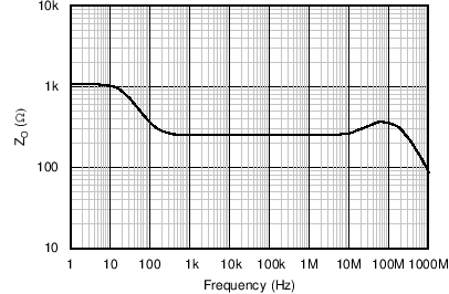
| ZO | Open-loop output impedance | VS = 5 V, f = 10 MHz | 250 | Ω | |||
| POWER SUPPLY | |||||||
| VS | Specified voltage | 1.8 | 5.5 | V | |||
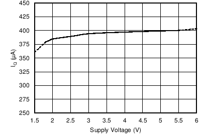
| IQ | Quiescent current per amplifier | VS = 5 V, IO = 0 mA, TA= –40°C to 125°C | 400 | 500 | µA | ||
| Power-on time | VS = 0 V to 5.5 V | 200 | µs | ||||
(1) Third-order filter; bandwidth = 80 kHz at –3 dB.
6.8 Typical Characteristics
at TA = 25°C, VS = 5.5 V, RL = 10 kΩ connected to VS / 2, VCM = VS / 2, and VOUT = VS / 2, unless otherwise noted.
| Distribution taken from 12551 amplifiers | ||

| 9 typical units shown | ||

| V+ = 0.9 V to 2.75 V, V– = –0.9 V to –2.75 V, 9 typical units shown |

| RL = 10 kΩ | ||


| V+ = 2.75 V, V– = –2.75 V | ||


| Bandwidth = 80 kHz, VOUT = 0.5 VRMS | ||


| V+ = 2.75 V | G = +1 V/V | RL = 1 kΩ |
| V– = –2.75 V |

| V+ = 2.75 V | V– = –2.75 V | G = –10 V/V |

| V+ = 2.75 V | V– = –2.75 V | G = +1 V/V |

| CL = 100 pF | G = +1 V/V |


| PRF = –10 dBm | ||
Referred to Noninverting Input (EMIRR IN+) vs Frequency

| TA = –40°C to +125°C, Distribution taken from 70 amplifiers | ||

| V+ = 2.75 V, V– = –2.75 V, 9 typical units shown | ||

| VCM < (V+) – 1.4 V | ||

| RL = 2 kΩ | ||


(Referred to Input)


| ƒ = 1 kHz | ||

| ƒ = 1 kHz, Bandwidth = 80 kHz | ||


| V+ = 2.75 V | V– = –2.75 V | G = –1 V/V |

| V+ = 2.75 V | V– = –2.75 V | |

| V+ = 2.75 V | V– = –2.75 V | G = –10 V/V |

| V+ = 2.75 V | CL = 100 pF | G = +1 V/V |
| V– = –2.75 V |

| CL = 100 pF | G = +1 V/V |

Frequency and Supply Voltage

| V+ = 2.75 V, V– = –2.75 V | ||