SBOSAE8B October 2023 – April 2024 OPA2323 , OPA323 , OPA4323
PRODMIX
- 1
- 1 Features
- 2 Applications
- 3 Description
- 4 Device Comparison Table
- 5 Pin Configuration and Functions
- 6 Specifications
-
7 Detailed Description
- 7.1 Overview
- 7.2 Functional Block Diagram
- 7.3
Feature Description
- 7.3.1 Operating Voltage
- 7.3.2 Rail-to-Rail Input
- 7.3.3 Rail-to-Rail Output
- 7.3.4 Common-Mode Rejection Ratio (CMRR)
- 7.3.5 Capacitive Load and Stability
- 7.3.6 Overload Recovery
- 7.3.7 EMI Rejection
- 7.3.8 ESD and Electrical Overstress
- 7.3.9 Input ESD Protection
- 7.3.10 Shutdown Function
- 7.3.11 Packages with an Exposed Thermal Pad
- 7.4 Device Functional Modes
- 8 Application and Implementation
- 9 Device and Documentation Support
- 10Revision History
- 11Mechanical, Packaging, and Orderable Information
Package Options
Refer to the PDF data sheet for device specific package drawings
Mechanical Data (Package|Pins)
- DCK|5
Thermal pad, mechanical data (Package|Pins)
Orderable Information
7.3.2 Rail-to-Rail Input
The input common-mode voltage range of the OPAx323 series extends beyond the supply rails with a common-mode rejection ratio (CMRR) of 100dB minimum at 5.5V as specified in Electrical Characteristics. The device is designed to have a good performance of 85dB minimum CMRR even when operating at an ultra-low supply voltage of 1.8V. This is made possible by using a zero-cross input stage architecture for the amplifier input pair.
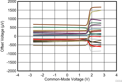
Most commercial amplifiers employ a complementary input stage architecture which often limits the rail-to-rail CMRR to less than 65dB. This is because the offset performance across the rail-to-rail input common-mode range is not linear. One of the input pairs, usually, the P-channel pair with better offset, noise performance is designed to cover the majority of the common-mode range with the N-channel pair slated to slowly take over at a certain threshold voltage from the positive rail. The creates a big jump in the offset voltage across common mode when transitioning across the input pairs as shown in TLV900x Offset Voltage vs Common-Mode. This offset jump not only affects CMRR but also limits linearity / THD for rail-to-rail input signals.
The OPAx323 achieves linear offset performance over the entire rail-to-rail input range by extending the common-mode-range of a single P-channel input pair using an internal charge pump as shown in the Functional Block Diagram. This eliminates the need for the N-channel input pair and the resulting offset jump caused by input pair transitions.
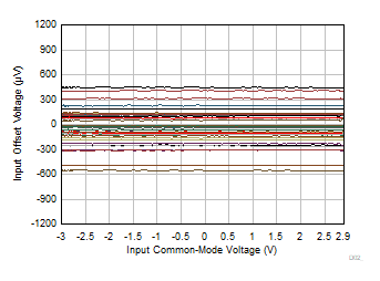
The OPAx323 exhibits near to zero shift in offset voltage across the entire common-mode voltage as shown in Figure 7-72. This is crucial to achieving high linearity in ADC driver and audio driver applications.

| V+ = 2.75V, V– = –2.75V | No. of devices = 45 |
| (V–) – 0.25V < VCM < (V+) + 0.15V | |

| V+ = 2.75V, V– = –2.75V |