SBOS465C January 2009 – January 2016 OPA2348-Q1 , OPA348-Q1 , OPA4348-Q1
PRODUCTION DATA.
- 1 Features
- 2 Applications
- 3 Description
- 4 Revision History
- 5 Pin Configuration and Functions
- 6 Specifications
- 7 Detailed Description
- 8 Application and Implementation
- 9 Power Supply Recommendations
- 10Layout
- 11Device and Documentation Support
- 12Mechanical, Packaging, and Orderable Information
Package Options
Mechanical Data (Package|Pins)
Thermal pad, mechanical data (Package|Pins)
Orderable Information
8 Application and Implementation
NOTE
Information in the following applications sections is not part of the TI component specification, and TI does not warrant its accuracy or completeness. TI’s customers are responsible for determining suitability of components for their purposes. Customers should validate and test their design implementation to confirm system functionality.
8.1 Application Information
The OPAx348-Q1 operational amplifiers (op amps) are unity-gain stable and suitable for a wide range of general-purpose applications.
The OPAx348-Q1 device features wide bandwidth and unity-gain stability with rail-to-rail input and output for increased dynamic range. Figure 23 shows the input and output waveforms for the OPAx348-Q1 device in unity-gain configuration. Operation is from a single 5-V supply with a 100-kΩ load connected to VS / 2. The input is a 5-VPP sinusoid. Output voltage is approximately 4.98 VPP.
The power-supply pins should be bypassed with 0.01-µF ceramic capacitors.
8.1.1 Driving Analog-to-Digital Converters (ADCs)
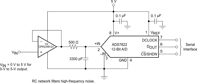
The OPAx348-Q1 op amps are optimized for driving medium-speed sampling ADCs. The OPAx348-Q1 op amps buffer the ADC input capacitance and resulting charge injection while providing signal gain.
Figure 26 shows the OPA2348 in a basic noninverting configuration driving the ADS7822 device. The ADS7822 device is a 12-bit, micropower sampling converter in the MSOP-8 package. When used with the low-power miniature packages of the OPAx348-Q1 family of devices, the combination is ideal for space-limited, low-power applications. In this configuration, an RC network at the ADC input can be used to provide for anti-aliasing filtering and charge injection current.

The OPAx348-Q1 family of devices can also be used in noninverting configuration to drive the ADS7822 device in limited low-power applications. In this configuration, an RC network at the ADC input can be used to provide for anti-aliasing filtering and charge injection current. See Figure 26 for the OPAx348-Q1 driving an ADS7822 device in a speech bandpass filtered data acquisition system. This small, low-cost solution provides the necessary amplification and signal conditioning to interface directly with an electret microphone. This circuit operates with VS = 2.7 V to 5 V with less than 250-µA typical quiescent current.

8.2 Typical Application
Some applications require differential signals. Figure 28 shows a simple circuit to convert a single-ended input of 0.1 V to 2.4 V into a differential output of ±2.3 V on a single 2.7-V supply. The output range is intentionally limited to maximize linearity. The circuit is composed of two amplifiers. One amplifier functions as a buffer and creates a voltage, VOUT+. The second amplifier inverts the input and adds a reference voltage to generate VOUT–. Both VOUT+ and VOUT– range from 0.1 V to 2.4 V. The difference, VDIFF, is the difference between VOUT+ and VOUT–. This configuration makes the differential output voltage range to be 2.3 V.
 Figure 28. Schematic for a Single-Ended Input to Differential Output Conversion
8.2.1 Design Requirements
The design requirements are as follows:
- Supply voltage: 2.7 V
- Reference voltage: 2.5 V
- Input: 0.1 V to 2.4 V
- Output differential: ±2.3 V
- Output common-mode voltage: 1.25 V
- Small-signal bandwidth: 1 MHz
8.2.2 Detailed Design Procedure
The circuit in Figure 28 takes a single-ended input signal, VIN, and generates two output signals, VOUT+ and VOUT– using two amplifiers and a reference voltage, VREF. VOUT+ is the output of the first amplifier and is a buffered version of the input signal, VIN (as shown in Equation 1). VOUT– is the output of the second amplifier which uses VREF to add an offset voltage to VIN and feedback to add inverting gain. The transfer function for VOUT– is given in Equation 2.


The differential output signal, VDIFF, is the difference between the two single-ended output signals, VOUT+ and VOUT–. Equation 3 shows the transfer function for VDIFF. By applying the conditions that R1 = R2 and R3 = R4, the transfer function is simplified into Equation 6. Using this configuration, the maximum input signal is equal to the reference voltage and the maximum output of each amplifier is equal to VREF. The differential output range is 2 × VREF. Furthermore, the common-mode voltage (VCM) is one half of VREF (see Equation 7).


8.2.2.1 Amplifier Selection
Linearity over the input range is key for good dc accuracy. The common-mode input range and output swing limitations determine the linearity. In general, an amplifier with rail-to-rail input and output swing is required. Bandwidth is a key concern for this design, so the OPAx348-Q1 family of devices is selected because its bandwidth is greater than the target of 1 MHz. The bandwidth and power ratio makes this device power-efficient, and the low offset and drift ensure good accuracy for moderate precision applications.
8.2.2.2 Passive Component Selection
Because the transfer function of VOUT– relies heavily upon resistors (R1, R2, R3, and R4), use resistors with low tolerances to maximize performance and minimize error. This design uses resistors with resistance values of 49.9 kΩ and tolerances of 0.1%. However, if the noise of the system is a key parameter, smaller resistance values (6 kΩ or lower) can be selected to keep the overall system noise low. This technique ensures that the noise from the resistors is lower than the amplifier noise.
8.2.3 Application Curves


