SBOS233G March   2002  – April 2018 OPA2354 , OPA354 , OPA4354

PRODUCTION DATA.  

  1. Features
  2. Applications
  3. Description
    1.     Device Images
      1.      Simplified Schematic
  4. Revision History
  5. Device Comparison Table
  6. Pin Configuration and Functions
    1.     Pin Functions: OPA354
    2.     Pin Functions: OPA2354
    3.     Pin Functions: OPA4354
  7. Specifications
    1. 7.1 Absolute Maximum Ratings
    2. 7.2 ESD Ratings
    3. 7.3 Recommended Operating Conditions
    4. 7.4 Thermal Information: OPA354
    5. 7.5 Thermal Information: OPA2354
    6. 7.6 Thermal Information: OPA4354
    7. 7.7 Electrical Characteristics: VS = 2.7 V to 5.5 V (Single-Supply)
    8. 7.8 Typical Characteristics
  8. Detailed Description
    1. 8.1 Overview
    2. 8.2 Functional Block Diagram
    3. 8.3 Feature Description
      1. 8.3.1 Operating Voltage
      2. 8.3.2 Rail-to-Rail Input
      3. 8.3.3 Rail-to-Rail Output
      4. 8.3.4 Output Drive
      5. 8.3.5 Video
      6. 8.3.6 Driving Analog-to-Digital converters
      7. 8.3.7 Capacitive Load and Stability
      8. 8.3.8 Wideband Transimpedance Amplifier
    4. 8.4 Device Functional Modes
  9. Application and Implementation
    1. 9.1 Application Information
    2. 9.2 Typical Application
      1. 9.2.1 Design Requirements
      2. 9.2.2 Detailed Design Procedure
        1. 9.2.2.1 Optimizing the Transimpedance Circuit
      3. 9.2.3 Application Curve
  10. 10Power Supply Recommendations
  11. 11Layout
    1. 11.1 Layout Guidelines
    2. 11.2 Layout Example
    3. 11.3 Power Dissipation
    4. 11.4 PowerPAD Thermally-Enhanced Package
    5. 11.5 PowerPAD Assembly Process
  12. 12Device and Documentation Support
    1. 12.1 Documentation Support
    2. 12.2 Related Links
    3. 12.3 Receiving Notification of Documentation Updates
    4. 12.4 Community Resources
    5. 12.5 Trademarks
    6. 12.6 Electrostatic Discharge Caution
    7. 12.7 Glossary
  13. 13Mechanical, Packaging, and Orderable Information

Package Options

Mechanical Data (Package|Pins)
Thermal pad, mechanical data (Package|Pins)
Orderable Information

Driving Analog-to-Digital converters

The OPAx354 series op amps offer 60 ns of settling time to 0.01%, making the series a good choice for driving high- and medium-speed sampling A/D converters and reference circuits. The OPAx354 series provide an effective means of buffering the
A/D converter input capacitance and resulting charge injection while providing signal gain. For applications requiring high DC accuracy, the OPA350 series is recommended.

Figure 34 shows the OPAx354 driving an A/D converter. With the OPAx354 in an inverting configuration, a capacitor across the feedback resistor is used to filter high-frequency noise in the signal.
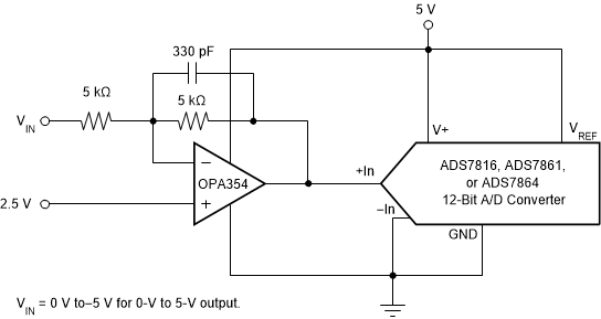
OPA354 OPA2354 OPA4354 ai_inverting_config_driving_adc_bos233.gif
A/D converter input = 0 V to VREF
Figure 34. The OPAx354 in Inverting Configuration Driving the ADS7816