SLOS868C December 2013 – May 2018 OPA355-Q1
PRODUCTION DATA.
- 1 Features
- 2 Applications
- 3 Description
- 4 Revision History
- 5 Device Comparison Table
- 6 Pin Configuration and Functions
- 7 Specifications
- 8 Detailed Description
- 9 Application and Implementation
- 10Power Supply Recommendations
- 11Layout
- 12Device and Documentation Support
- 13Mechanical, Packaging, and Orderable Information
Package Options
Refer to the PDF data sheet for device specific package drawings
Mechanical Data (Package|Pins)
- DBV|6
Thermal pad, mechanical data (Package|Pins)
Orderable Information
3 Description
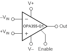
The OPA355-Q1 device is a high-speed, voltage-feedback CMOS operational amplifier designed for applications requiring wide bandwidth. The OPA355-Q1 device is unity-gain stable and can drive large output currents. In addition, the OPA355-Q1 device has a digital shutdown (enable) function. This feature provides power saving during idle periods and places the output in a high-impedance state to support output multiplexing. The differential gain is 0.02% and the differential phase is 0.05°. The quiescent current is 8.3 mA per channel.
The OPA355-Q1 device is optimized for operation on single supply or dual supplies as low as 2.5 V (±1.25 V) and up to 5.5 V (±2.75 V). The common-mode input range for the OPA355-Q1 device extends 100 mV below ground and up to 1.5 V from V+. The output swing is within 100 mV of the rails, supporting wide dynamic range.
The OPA355-Q1 device is available in a single SOT-23-6 package and is specified over the extended –40°C to +125°C temperature range.
Device Information(1)
| PART NUMBER | PACKAGE | BODY SIZE (NOM) |
|---|---|---|
| OPA355-Q1 | SOT-23 (6) | 2.90 mm × 1.60 mm |
- For all available packages, see the orderable addendum at the end of the data sheet.
