SLOS868C December 2013 – May 2018 OPA355-Q1
PRODUCTION DATA.
- 1 Features
- 2 Applications
- 3 Description
- 4 Revision History
- 5 Device Comparison Table
- 6 Pin Configuration and Functions
- 7 Specifications
- 8 Detailed Description
- 9 Application and Implementation
- 10Power Supply Recommendations
- 11Layout
- 12Device and Documentation Support
- 13Mechanical, Packaging, and Orderable Information
Package Options
Refer to the PDF data sheet for device specific package drawings
Mechanical Data (Package|Pins)
- DBV|6
Thermal pad, mechanical data (Package|Pins)
Orderable Information
9.2.2 High-Impedance Sensor Interface
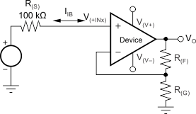
Many sensors have high source impedances that may range up to 10 MΩ, or even higher. The output signal of sensors often must be amplified or otherwise conditioned by means of an amplifier. The input bias current of this amplifier can load the sensor output and cause a voltage drop across the source resistance, as shown in Figure 34, where (V(+INx) = VS – I(BIAS) × R(S)). The last term, I(BIAS) × R(S), shows the voltage drop across R(S). To prevent errors introduced to the system as a result of this voltage, an op amp with very low input bias current must be used with high impedance sensors. This low current keeps the error contribution by I(BIAS) × R(S) less than the input voltage noise of the amplifier, so that it does not become the dominant noise factor. The OPA355-Q1 op amp features very low input bias current (typically 200 fA), and is therefore a preferred choice for such applications.
 Figure 34. Noise as a Result of I(BIAS)