SBOS235F March 2002 – April 2018 OPA2357 , OPA357
PRODUCTION DATA.
- 1 Features
- 2 Applications
- 3 Description
- 4 Revision History
- 5 Pin Configuration and Functions
- 6 Specifications
-
7 Detailed Description
- 7.1 Overview
- 7.2 Functional Block Diagram
- 7.3
Feature Description
- 7.3.1 OPAx357 Comparison
- 7.3.2 Operating Voltage
- 7.3.3 Enable Function
- 7.3.4 Rail-to-Rail Input
- 7.3.5 Rail-to-Rail Output
- 7.3.6 Output Drive
- 7.3.7 Video
- 7.3.8 Wideband Video Multiplexing
- 7.3.9 Driving Analog-to-Digital Converters
- 7.3.10 Capacitive Load and Stability
- 7.3.11 Wideband Transimpedance Amplifier
- 7.4 Device Functional Modes
- 8 Application and Implementation
- 9 Power Supply Recommendations
- 10Layout
- 11Device and Documentation Support
- 12Mechanical, Packaging, and Orderable Information
Package Options
Mechanical Data (Package|Pins)
- DBV|6
Thermal pad, mechanical data (Package|Pins)
Orderable Information
5 Pin Configuration and Functions
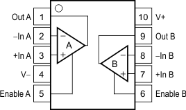
OPA2357: DGS Package
10-Pin VSSOP
Top View

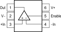
1. Pin 1 of the SOT23-6 is determined by orienting the package marking as indicated in the diagram.
Pin Functions
| PIN | I/O | DESCRIPTION | ||
|---|---|---|---|---|
| NAME | DBV
(SOT-23) |
DGS (VSSOP) | ||
| Enable | 5 | — | — | Amplifier power down.
Low = disabled, high = normal operation (pin must be driven). |
| Enable A | — | 5 | — | Amplifier power down, channel A.
Low = disabled, high = normal operation (pin must be driven). |
| Enable B | — | 6 | — | Amplifier power down, channel B.
Low = disabled, high = normal operation (pin must be driven). |
| –In | 4 | — | I | Inverting input pin |
| –In A | — | 2 | I | Inverting input pin, channel A |
| –In B | — | 8 | I | Inverting input pin, channel B |
| +In | 3 | — | I | Noninverting input pin |
| +In A | — | 3 | I | Noninverting input pin, channel A |
| +In B | — | 7 | I | Noninverting input pin, channel B |
| Out | 1 | — | O | Output pin |
| Out A | — | 1 | O | Output pin, channel A |
| Out B | — | 9 | O | Output pin, channel B |
| V– | 2 | 4 | — | Negative power supply |
| V+ | 6 | 10 | — | Positive power supply |
