SBOS235F March   2002  – April 2018 OPA2357 , OPA357

PRODUCTION DATA.  

  1. Features
  2. Applications
  3. Description
    1.     Device Images
      1.      Simplified Schematic
  4. Revision History
  5. Pin Configuration and Functions
    1.     Pin Functions
  6. Specifications
    1. 6.1 Absolute Maximum Ratings
    2. 6.2 ESD Ratings
    3. 6.3 Recommended Operating Conditions
    4. 6.4 Thermal Information
    5. 6.5 Electrical Characteristics: VS = +2.7-V to +5.5-V Single-Supply
    6. 6.6 Typical Characteristics
  7. Detailed Description
    1. 7.1 Overview
    2. 7.2 Functional Block Diagram
    3. 7.3 Feature Description
      1. 7.3.1  OPAx357 Comparison
      2. 7.3.2  Operating Voltage
      3. 7.3.3  Enable Function
      4. 7.3.4  Rail-to-Rail Input
      5. 7.3.5  Rail-to-Rail Output
      6. 7.3.6  Output Drive
      7. 7.3.7  Video
      8. 7.3.8  Wideband Video Multiplexing
      9. 7.3.9  Driving Analog-to-Digital Converters
      10. 7.3.10 Capacitive Load and Stability
      11. 7.3.11 Wideband Transimpedance Amplifier
    4. 7.4 Device Functional Modes
  8. Application and Implementation
    1. 8.1 Application Information
    2. 8.2 Typical Applications
      1. 8.2.1 Transimpedance Amplifier
        1. 8.2.1.1 Design Requirements
        2. 8.2.1.2 Detailed Design Procedure
          1. 8.2.1.2.1 Custom Design With WEBENCH® Tools
          2. 8.2.1.2.2 OPAx357 Design Procedure
            1. 8.2.1.2.2.1 Optimizing the Transimpedance Circuit
        3. 8.2.1.3 Application Curve
      2. 8.2.2 High-Impedance Sensor Interface
      3. 8.2.3 Driving ADCs
      4. 8.2.4 Active Filter
  9. Power Supply Recommendations
    1. 9.1 Power Dissipation
  10. 10Layout
    1. 10.1 Layout Guidelines
    2. 10.2 Layout Example
  11. 11Device and Documentation Support
    1. 11.1 Device Support
      1. 11.1.1 Development Support
        1. 11.1.1.1 Custom Design With WEBENCH® Tools
    2. 11.2 Documentation Support
      1. 11.2.1 Related Documentation
    3. 11.3 Related Links
    4. 11.4 Receiving Notification of Documentation Updates
    5. 11.5 Community Resources
    6. 11.6 Trademarks
    7. 11.7 Electrostatic Discharge Caution
    8. 11.8 Glossary
  12. 12Mechanical, Packaging, and Orderable Information

Package Options

Mechanical Data (Package|Pins)
Thermal pad, mechanical data (Package|Pins)
Orderable Information

Typical Characteristics

at TA = 25°C, VS = 5 V, G = +1, RF = 0 Ω, RL = 1 kΩ, and connected to VS / 2 (unless otherwise noted)
OPA357 OPA2357 OPA357_SBOS235_G001.gif
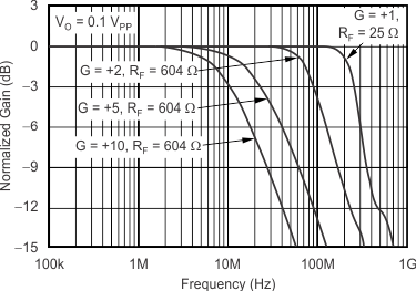
Figure 1. Noninverting Small-Signal Frequency Response
OPA357 OPA2357 OPA357_SBOS235_G003.gif
Figure 3. Noninverting Small-Signal Step Response
OPA357 OPA2357 OPA357_SBOS235_G005.gif
Figure 5. Large-Signal Disable, Enable Response
OPA357 OPA2357 OPA357_SBOS235_G007.gif
Figure 7. Harmonic Distortion vs Output Voltage
OPA357 OPA2357 OPA357_SBOS235_G009.gif
Figure 9. Harmonic Distortion vs Inverting Gain
OPA357 OPA2357 OPA357_SBOS235_G011.gif
Figure 11. Harmonic Distortion vs Load Resistance
OPA357 OPA2357 OPA357_SBOS235_G013.gif
Figure 13. Frequency Response for Various RL
OPA357 OPA2357 OPA357_SBOS235_G015.gif
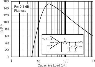
Figure 15. Recommended RS vs Capacitive Load
OPA357 OPA2357 OPA357_SBOS235_G017.gif
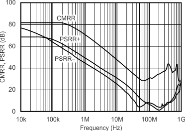
Figure 17. Common-Mode Rejection Ratio and Power-Supply Rejection Ratio vs Frequency
OPA357 OPA2357 OPA357_SBOS235_G019.gif
Figure 19. Composite Video differential Gain and Phase
OPA357 OPA2357 OPA357_SBOS235_G021.gif
VS = 3 V
Figure 21. Output Voltage Swing vs Output Current
OPA357 OPA2357 OPA357_SBOS235_G023.gif
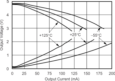
VS = 5 V
Figure 23. Output Voltage Swing vs Output Current
OPA357 OPA2357 OPA357_SBOS235_G025.gif
Figure 25. Disable Feedthrough vs Frequency
OPA357 OPA2357 OPA357_SBOS235_G027.gif
Figure 27. Maximum Output Voltage vs Frequency
OPA357 OPA2357 OPA357_SBOS235_G029.gif
Figure 29. Open-Loop Gain vs Temperature
OPA357 OPA2357 OPA357_SBOS235_G031.gif
Figure 31. Common-Mode Rejection Ratio and Power-Supply Rejection Ratio vs Temperature
OPA357 OPA2357 OPA357_SBOS235_G002.gif
Figure 2. Inverting Small-Signal Frequency Response
OPA357 OPA2357 OPA357_SBOS235_G004.gif
Figure 4. Noninverting Large-Signal Step Response
OPA357 OPA2357 OPA357_SBOS235_G006.gif
Figure 6. 0.1-dB Gain Flatness
OPA357 OPA2357 OPA357_SBOS235_G008.gif
Figure 8. Harmonic Distortion vs Noninverting Gain
OPA357 OPA2357 OPA357_SBOS235_G010.gif
Figure 10. Harmonic Distortion vs Frequency
OPA357 OPA2357 OPA357_SBOS235_G012.gif
Figure 12. Input Voltage and Current Noise Spectral Density vs Frequency
OPA357 OPA2357 OPA357_SBOS235_G014.gif
Figure 14. Frequency Response for Various CL
OPA357 OPA2357 OPA357_SBOS235_G016.gif
Figure 16. Frequency Response vs Capacitive Load
OPA357 OPA2357 OPA357_SBOS235_G018.gif
Figure 18. Open-Loop Gain and Phase
OPA357 OPA2357 OPA357_SBOS235_G020.gif
Figure 20. Input Bias Current vs Temperature
OPA357 OPA2357 OPA357_SBOS235_G022.gif
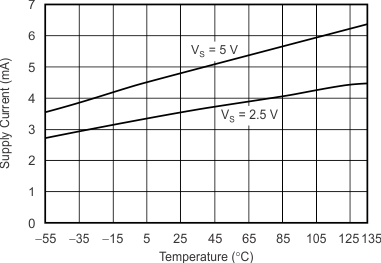
Figure 22. Supply Current vs Temperature
OPA357 OPA2357 OPA357_SBOS235_G024.gif
Figure 24. Shutdown Current vs Temperature
OPA357 OPA2357 OPA357_SBOS235_G026.gif
Figure 26. Closed-Loop Output Impedance vs Frequency
OPA357 OPA2357 OPA357_SBOS235_G028.gif
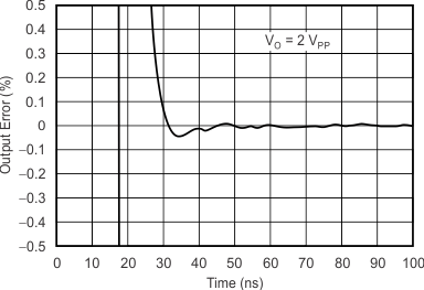
Figure 28. Output Settling Time to 0.1%
OPA357 OPA2357 OPA357_SBOS235_G030.gif
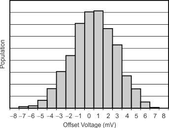
Figure 30. Offset Voltage Production Distribution
OPA357 OPA2357 OPA357_SBOS235_G032.gif
Figure 32. Channel-to-Channel Crosstalk