SBOS937D October 2020 – December 2023 OPA3S328
PRODUCTION DATA
- 1
- 1 Features
- 2 Applications
- 3 Description
- 4 Pin Configuration and Functions
- 5 Specifications
- 6 Parameter Measurement Information
- 7 Detailed Description
- 8 Application and Implementation
- 9 Device and Documentation Support
- 10Revision History
- 11Mechanical, Packaging, and Orderable Information
Package Options
Mechanical Data (Package|Pins)
Thermal pad, mechanical data (Package|Pins)
- RGR|20
Orderable Information
3 Description
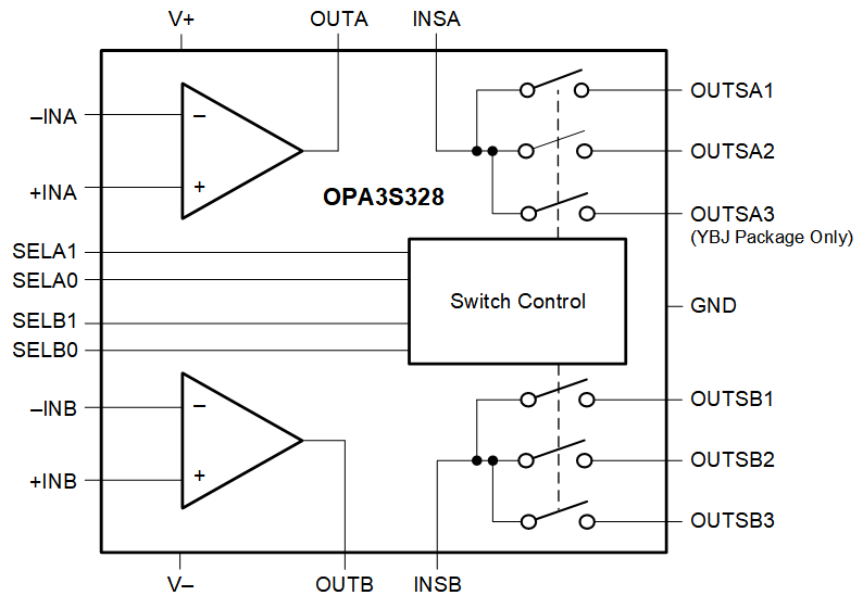
The OPA3S328 is a precision, low-voltage, CMOS operational amplifier (op amp) with integrated switches that are optimized for flexible transimpedance applications. Low input bias current and low input capacitance allows for high-frequency transimpedance gains at low photocurrent operation (< 1 nA). The integrated switches, low offset, and rail-to-rail output performance of the OPA3S328 enable high accuracy across multiple decades of current values. Small packages, along with integrated switches, allow for selectable transimpedance gains and help reduce size for space-constrained applications.
The OPA3S328 features zero-crossover input technology, giving the flexibility for the input common-mode range to span the full supply range without offset deviations. The device provides enable-disable capability to allow for portable, handheld applications in test and measurement. When disabled, the OPA3S328 output impedance is typically 100 GΩ, allowing for wired-OR applications using multiple transimpedance channels.
| PART NUMBER | PACKAGE(1) | PACKAGE SIZE(2) |
|---|---|---|
| OPA3S328 | RGR (VQFN, 20) | 3.5 mm × 3.5 mm |
| YBJ (DSBGA, 24) | 2 mm × 2 mm |
 Functional Block Diagram
 Input
Offset Voltage vs Input Common-Mode Voltage