-
OPAx170-Q1 36-V, Single-Supply, Low-Power, Automotive-Grade Operational Amplifiers SBOS834B December 2016 – November 2017 OPA170-Q1 , OPA2170-Q1 , OPA4170-Q1
PRODUCTION DATA.
-
OPAx170-Q1 36-V, Single-Supply, Low-Power, Automotive-Grade Operational Amplifiers
- 1 Features
- 2 Applications
- 3 Description
- 4 Revision History
- 5 Pin Configuration and Functions
- 6 Specifications
- 7 Detailed Description
- 8 Application and Implementation
- 9 Power Supply Recommendations
- 10Layout
- 11Device and Documentation Support
- 12Mechanical, Packaging, and Orderable Information
- IMPORTANT NOTICE
Package Options
Mechanical Data (Package|Pins)
- PW|14
Thermal pad, mechanical data (Package|Pins)
Orderable Information
OPAx170-Q1 36-V, Single-Supply, Low-Power, Automotive-Grade Operational Amplifiers
1 Features
- Qualified for Automotive Applications
- AEC-Q100 Qualified With the Following Results:
- Device Temperature Grade 1: –40°C to +125°C Ambient Operating Temperature
- Device HBM ESD Classification Level 3A
- Device CDM ESD Classification Level C5
- Supply Range: 2.7 V to 36 V, ±1.35 V to ±18 V
- Low Noise: 19 nV/√Hz
- RFI Filtered Inputs
- Input Range Includes the Negative Supply
- Input Range Operates to Positive Supply
- Rail-to-Rail Output
- Gain Bandwidth: 1.2 MHz
- Low Quiescent Current: 110 µA per Amplifier
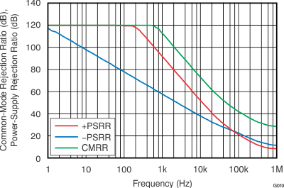
- High Common-Mode Rejection: 120 dB
- Low Bias Current: 15 pA (Maximum)
- Number of Channels:
- OPA170-Q1: 1
- OPA2170-Q1: 2
- OPA4170-Q1: 4
- Industry-Standard Packages
2 Applications
- Automotive
- HEV and EV Power Trains
- Advanced Driver Assist (ADAS)
- Automatic Climate Controls
- Temperature Measurements
- Strain Gauge Amplifiers
- Precision Integrators
3 Description
The OPA170-Q1, OPA2170-Q1, and OPA4170-Q1 devices (OPAx170-Q1) are a family of 36-V, single-supply, low-noise operational amplifiers that feature micro packages with the ability to operate on supplies ranging from 2.7 V (±1.35 V) to 36 V (±18 V). They offer good offset, drift, and bandwidth with low quiescent current.
Unlike most operational amplifiers, which are specified at only one supply voltage, the OPAx170-Q1 family of operational amplifiers is specified from 2.7 V to 36 V. Input signals beyond the supply rails do not cause phase reversal. The OPAx170-Q1 family is stable with capacitive loads up to 300 pF. The input can operate 100 mV below the negative rail and within 2 V of the positive rail for normal operation. Note that these devices can operate with full rail-to-rail input 100 mV beyond the positive rail, but with reduced performance within 2 V of the positive rail. The OPAx170-Q1 operational amplifiers are specified from –40°C to +125°C.
Device Information(1)
| PART NUMBER | PACKAGE | BODY SIZE (NOM) |
|---|---|---|
| OPA170-Q1 | SOT-23 (5) | 2.90 mm × 1.60 mm |
| OPA2170-Q1 | VSSOP (8) | 3.00 mm × 3.00 mm |
| OPA4170-Q1 | TSSOP (14) | 5.00 mm × 4.40 mm |
- For all available packages, see the orderable addendum at the end of the data sheet.
4 Revision History
Changes from A Revision (March 2017) to B Revision
- Deleted 8-pin SOIC, 5-pin SOT, 8-pin VSSOP, and 14-pin SOIC packages from Device Information tableGo
- Changed front-page graphic Go
- Deleted OPA170-Q1 D (SOIC) and DRL (SOT) pinout drawings and pinout table informationGo
- Deleted OPA2170-Q1 D (SOIC) and DCU (VSSOP Micro size packagesGo
- Deleted OPA170-Q1 D (SOIC) pinout drawingGo
- Deleted D (SOIC) and DRL (SOT) thermal information from OPA170-Q1 Thermal Information table Go
- Deleted D (SOIC) and DCU (VSSOP) thermal information from OPA2170-Q1 Thermal Information table Go
- Deleted D (SOIC) thermal information from OPA4170-Q1 Thermal Information table Go
- Changed values in Figure 38 from 250 Ω to 2.5 kΩ Go
Changes from * Revision (December 2016) to A Revision
- Deleted last sentence of first para of Description Go
- Deleted static literature number in Thermal Information: OPA170-Q1 table note Go
- Separated the IB and IOS test conditions for the OPA4170 in Electrical Characteristics tableGo
- Added additional text to Figure 8 title Go
- Changed "many specifications apply from –40°C to +125°C" to "many specifications apply from –40°C to +85°C" to correct typoGo
5 Pin Configuration and Functions

Table 1. Pin Functions: OPA170-Q1
| PIN | I/O | DESCRIPTION | |
|---|---|---|---|
| NAME | NO. | ||
| IN– (–IN) | 4 | I | Negative (inverting) input |
| IN+ (+IN) | 3 | I | Positive (noninverting) input |
| OUT | 1 | O | Output |
| V– | 2 | — | Negative (lowest) power supply |
| V+ | 5 | — | Positive (highest) power supply |
Table 2. Pin Functions: OPA2170-Q1
| PIN | I/O | DESCRIPTION | |
|---|---|---|---|
| NAME | NO. | ||
| –IN A | 2 | I | Inverting input, channel A |
| –IN B | 6 | I | Inverting input, channel B |
| +IN A | 3 | I | Noninverting input, channel A |
| +IN B | 5 | I | Noninverting input, channel B |
| OUT A | 1 | O | Output, channel A |
| OUT B | 7 | O | Output, channel B |
| V– | 4 | — | Negative (lowest) power supply |
| V+ | 8 | — | Positive (highest) power supply |
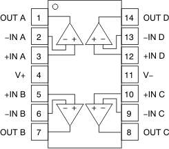
Table 3. Pin Functions: OPA4170-Q1
| PIN | I/O | DESCRIPTION | |
|---|---|---|---|
| NAME | NO. | ||
| –IN A | 2 | I | Inverting input, channel A |
| –IN B | 6 | I | Inverting input, channel B |
| –IN C | 9 | I | Inverting input, channel C |
| –IN D | 13 | I | Inverting input, channel D |
| +IN A | 3 | I | Noninverting input, channel A |
| +IN B | 5 | I | Noninverting input, channel B |
| +IN C | 10 | I | Noninverting input, channel C |
| +IN D | 12 | I | Noninverting input, channel D |
| OUT A | 1 | O | Output, channel A |
| OUT B | 7 | O | Output, channel B |
| OUT C | 8 | O | Output, channel C |
| OUT D | 14 | O | Output, channel D |
| V– | 11 | — | Negative (lowest) power supply |
| V+ | 4 | — | Positive (highest) power supply |
6 Specifications
6.1 Absolute Maximum Ratings
over operating free-air temperature range (unless otherwise noted)(1)| MIN | MAX | UNIT | |
|---|---|---|---|
| Supply voltage | –20 | 20 | V |
| Single supply voltage | 40 | V | |
| Signal input pin voltage | (V–) – 0.5 | (V+) + 0.5 | V |
| Signal input pin current | –10 | 10 | mA |
| Output short-circuit current(2) | Continuous | ||
| Operating ambient temperature, TA | –55 | 150 | °C |
| Junction temperature, TJ | 150 | °C | |
| Storage temperature, Tstg | –65 | 150 | °C |
6.2 ESD Ratings
| VALUE | UNIT | |||
|---|---|---|---|---|
| V(ESD) | Electrostatic discharge | Human-body model (HBM), per AEC Q100-002(1) | ±4000 | V |
| Charged-device model (CDM), per AEC Q100-011 | ±750 | |||
6.3 Recommended Operating Conditions
over operating free-air temperature range (unless otherwise noted)| MIN | MAX | UNIT | ||
|---|---|---|---|---|
| VS | Supply voltage (V+ – V–) | 2.7 | 36 | V |
| TA | Operating temperature | –40 | 125 | °C |
6.4 Thermal Information: OPA170-Q1
| THERMAL METRIC(1) | OPA170-Q1 | UNIT | |
|---|---|---|---|
| DBV (SOT-23) | |||
| 5 PINS | |||
| RθJA | Junction-to-ambient thermal resistance | 245.8 | °C/W |
| RθJC(top) | Junction-to-case (top) thermal resistance | 133.9 | °C/W |
| RθJB | Junction-to-board thermal resistance | 83.6 | °C/W |
| ψJT | Junction-to-top characterization parameter | 18.2 | °C/W |
| ψJB | Junction-to-board characterization parameter | 83.1 | °C/W |
| RθJC(bot) | Junction-to-case (bottom) thermal resistance | — | °C/W |
6.5 Thermal Information: OPA2170-Q1
| THERMAL METRIC(1) | OPA2170-Q1 | UNIT | |
|---|---|---|---|
| DGK (VSSOP) | |||
| 8 PINS | |||
| RθJA | Junction-to-ambient thermal resistance | 180 | °C/W |
| RθJC(top) | Junction-to-case (top) thermal resistance | 55 | °C/W |
| RθJB | Junction-to-board thermal resistance | 130 | °C/W |
| ψJT | Junction-to-top characterization parameter | 5.3 | °C/W |
| ψJB | Junction-to-board characterization parameter | 120 | °C/W |
| RθJC(bot) | Junction-to-case (bottom) thermal resistance | — | °C/W |
6.6 Thermal Information: OPA4170-Q1
| THERMAL METRIC(1) | OPA4170-Q1 | UNIT | |
|---|---|---|---|
| PW (TSSOP) | |||
| 14 PINS | |||
| RθJA | Junction-to-ambient thermal resistance | 106.9 | °C/W |
| RθJC(top) | Junction-to-case (top) thermal resistance | 24.4 | °C/W |
| RθJB | Junction-to-board thermal resistance | 59.3 | °C/W |
| ψJT | Junction-to-top characterization parameter | 0.6 | °C/W |
| ψJB | Junction-to-board characterization parameter | 54.3 | °C/W |
| RθJC(bot) | Junction-to-case (bottom) thermal resistance | — | °C/W |
6.7 Electrical Characteristics
at TA = 25°C, VCM = VOUT = VS / 2, and RL = 10 kΩ connected to VS / 2 (unless otherwise noted)| PARAMETER | TEST CONDITIONS | MIN | TYP | MAX | UNIT | |
|---|---|---|---|---|---|---|
| OFFSET VOLTAGE | ||||||
| VOS | Input offset voltage | TA = 25°C | 0.25 | ±1.8 | mV | |
| TA = –40°C to 125°C | ±2 | mV | ||||
| dVOS/dT | Input offset voltage drift | TA = –40°C to 125°C | ±0.3 | ±2 | µV/°C | |
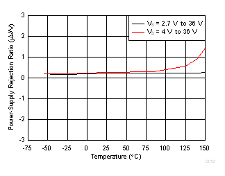
| PSRR | Input offset voltage vs power supply | VS = 4 V to 36 V TA = –40°C to 125°C |
1 | ±5 | µV/V | |
| Channel separation, dc | 5 | µV/V | ||||
| INPUT BIAS CURRENT | ||||||
| IB | Input bias current | TA = 25°C | ±8 | ±15 | pA | |
| TA = –40°C to 125°C (OPA170-Q1 and OPA2170-Q1) | ±3.5 | nA | ||||
| TA = –40°C to 125°C (OPA4170-Q1) | ±16 | |||||
| IOS | Input offset current | TA = 25°C | ±4 | ±15 | pA | |
| TA = –40°C to 125°C (OPA170-Q1 and OPA2170-Q1) | ±3.5 | nA | ||||
| TA = –40°C to 125°C (OPA4170-Q1) | ±16 | |||||
| NOISE | ||||||
| Input voltage noise | ƒ = 0.1 Hz to 10 Hz | 2 | µVPP | |||
| en | Input voltage noise density | ƒ = 100 Hz | 22 | nV/√Hz | ||
| ƒ = 1 kHz | 19 | nV/√Hz | ||||
| INPUT VOLTAGE | ||||||
| VCM | Common-mode voltage range(1) | (V–) – 0.1 | (V+) – 2 | V | ||
| CMRR | Common-mode rejection ratio | VS = ±2 V, (V–) – 0.1 V < VCM < (V+) – 2 V TA = –40°C to 125°C |
90 | 104 | dB | |
| VS = ±18 V, (V–) – 0.1 V < VCM < (V+) – 2 V TA = –40°C to 125°C |
104 | 120 | dB | |||
| INPUT IMPEDANCE | ||||||
| Differential | 100 || 3 | MΩ || pF | ||||
| Common-mode | 6 || 3 | 1012 Ω || pF | ||||
| OPEN-LOOP GAIN | ||||||
| AOL | Open-loop voltage gain | VS = 4 V to 36 V (V–) + 0.35 V < VO < (V+) – 0.35 V TA = –40°C to 125°C |
110 | 130 | dB | |
| FREQUENCY RESPONSE | ||||||
| GBP | Gain bandwidth product | 1.2 | MHz | |||
| SR | Slew rate | G = 1 | 0.4 | V/µs | ||
| tS | Settling time | To 0.1%, VS = ±18 V, G = 1 10-V step | 20 | µs | ||
| To 0.01% (12-bit), VS = ±18 V, G = 1 10-V step |
28 | µs | ||||
| Overload recovery time | VIN × Gain > VS | 2 | µs | |||
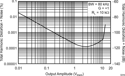
| THD+N | Total harmonic distortion + noise | G = 1, ƒ = 1 kHz, VO = 3 VRMS | 0.0002% | |||
| OUTPUT | ||||||
| VO | Voltage output swing from positive rail | IL = 0 mA VS = 4 V to 36 V |
10 | mV | ||
| IL sourcing 1 mA VS = 4 V to 36 V |
115 | mV | ||||
| VO | Voltage output swing from negative rail | IL = 0 mA VS = 4 V to 36 V |
8 | mV | ||
| IL sinking 1 mA VS = 4 V to 36 V |
70 | mV | ||||
| VO | Voltage output swing from rail | VS = 5 V RL = 10 kΩ TA = –40°C to 125°C |
(V–) + 0.03 | (V+) – 0.05 | V | |
| RL = 10 kΩ AOL ≥ 110 dB TA = –40°C to 125°C |
(V–) + 0.35 | (V+) – 0.35 | V | |||
| ISC | Short-circuit current | –20 | 17 | mA | ||
| CLOAD | Capacitive load drive | See Typical Characteristics | pF | |||
| RO | Open-loop output resistance | ƒ = 1 MHz IO = 0 A |
900 | Ω | ||
| POWER SUPPLY | ||||||
| VS | Specified voltage range | 2.7 | 36 | V | ||
| IQ | Quiescent current per amplifier | IO = 0 A TA = 25°C |
110 | 145 | µA | |
| IO = 0 A TA = –40°C to 125°C |
155 | µA | ||||
| TEMPERATURE | ||||||
| Specified range | –40 | 125 | °C | |||
| Operating range | –55 | 150 | °C | |||
6.8 Typical Characteristics: Table of Graphs
Table 4. Characteristic Performance Measurements
| DESCRIPTION | FIGURE |
|---|---|
| Offset Voltage Production Distribution | Figure 1 |
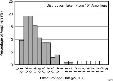
| Offset Voltage Drift Distribution | Figure 2 |
| Offset Voltage vs Temperature | Figure 3 |
| Offset Voltage vs Common-Mode Voltage | Figure 4 |
| Offset Voltage vs Common-Mode Voltage (Upper Stage) | Figure 5 |
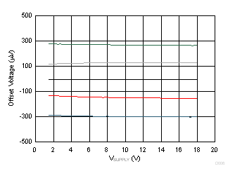
| Offset Voltage vs Power Supply | Figure 6 |
| IB and IOS vs Common-Mode Voltage | Figure 7 |
| Input Bias Current vs Temperature | Figure 8 |
| Output Voltage Swing vs Output Current (Maximum Supply) | Figure 9 |
| CMRR and PSRR vs Frequency (Referred-to-Input) | Figure 10 |
| CMRR vs Temperature | Figure 11 |
| PSRR vs Temperature | Figure 12 |
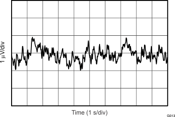
| 0.1-Hz to 10-Hz Noise | Figure 13 |
| Input Voltage Noise Spectral Density vs Frequency | Figure 14 |
| THD+N Ratio vs Frequency | Figure 15 |
| THD+N vs Output Amplitude | Figure 16 |
| Quiescent Current vs Temperature | Figure 17 |
| Quiescent Current vs Supply Voltage | Figure 18 |
| Open-Loop Gain and Phase vs Frequency | Figure 19 |
| Closed-Loop Gain vs Frequency | Figure 20 |
| Open-Loop Gain vs Temperature | Figure 21 |
| Open-Loop Output Impedance vs Frequency | Figure 22 |
| Small-Signal Overshoot vs Capacitive Load (100-mV Output Step) | Figure 23, Figure 24 |
| No Phase Reversal | Figure 25 |
| Positive Overload Recovery | Figure 26 |
| Negative Overload Recovery | Figure 27 |
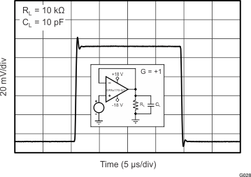
| Small-Signal Step Response (100 mV) | Figure 28, Figure 29 |
| Large-Signal Step Response | Figure 30, Figure 31 |
| Large-Signal Settling Time (10-V Positive Step) | Figure 32 |
| Large-Signal Settling Time (10-V Negative Step) | Figure 33 |
| Short-Circuit Current vs Temperature | Figure 34 |
| Maximum Output Voltage vs Frequency | Figure 35 |
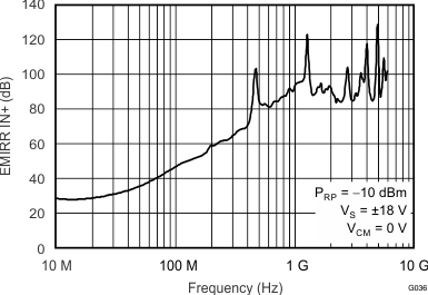
| EMIRR IN+ vs Frequency | Figure 36 |
6.9 Typical Characteristics
VS = ±18 V, VCM = VS / 2, RLOAD = 10 kΩ connected to VS / 2, and CL = 100 pF (unless otherwise noted)


(Upper Stage)




| 100-mV output step |


| 10-V negative step | ||


(Referred to Input)



| 100-mV output step |

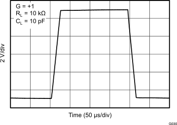

| 10-V positive step | ||

| 10-V negative step | ||
7 Detailed Description
7.1 Overview
The OPAx170-Q1 family of operational amplifiers provides high overall performance, making them ideal for many general-purpose applications. The excellent offset drift of only 2 μV/°C provides excellent stability over the entire temperature range. In addition, the device offers very good overall performance with high CMRR, PSRR, and AOL.
7.2 Functional Block Diagram

7.3 Feature Description
7.3.1 Operating Characteristics
The OPAx170-Q1 family of amplifiers is specified for operation from 2.7 V to 36 V (±1.35 V to ±18 V). Many of the specifications apply from –40°C to +125°C. Parameters that can exhibit significant variance with regard to operating voltage or temperature are listed in Table 4.
7.3.2 Phase-Reversal Protection
The OPAx170-Q1 family has an internal phase-reversal protection. Many operational amplifiers exhibit a phase reversal when the input is driven beyond the linear common-mode range. This condition is most often encountered in noninverting circuits when the input is driven beyond the specified common-mode voltage range, causing the output to reverse into the opposite rail. The input of the OPAx170-Q1 prevents phase reversal with excessive common-mode voltage. Instead, the output limits into the appropriate rail. Figure 37 shows this performance.
 Figure 37. No Phase Reversal
7.3.3 Electrical Overstress
Designers typically ask questions about the capability of an operational amplifier to withstand electrical overstress. These questions typically focus on the device inputs, but may involve the supply voltage pins or the output pin. Each of these different pin functions have electrical stress limits determined by the voltage breakdown characteristics of the particular semiconductor fabrication process and specific circuits connected to the pin. Internal electrostatic discharge (ESD) protection is built into these circuits to protect them from accidental ESD events both before and during product assembly.
A good understanding of basic ESD circuitry and the relevance of the circuitry to an electrical overstress event is helpful. Figure 38 shows the ESD circuits (indicated by the dashed line area) in the OPAx170-Q1. The ESD protection circuitry involves several current-steering diodes connected from the input and output pins and routed back to the internal power-supply lines, where the diodes meet at an absorption device internal to the operational amplifier. This protection circuitry is intended to remain inactive during normal circuit operation.
An ESD event produces a short-duration, high-voltage pulse that is transformed into a short-duration, high-current pulse when discharging through a semiconductor device. The ESD protection circuits are designed to provide a current path around the operational amplifier core to prevent damage. The energy absorbed by the protection circuitry is then dissipated as heat.
When an ESD voltage develops across two or more amplifier device pins, current flows through one or more steering diodes. The absorption device can activate depending on the path of the current. The absorption device has a trigger (or threshold voltage) that is above the normal operating voltage of the OPAx170-Q1, but below the device breakdown voltage level. When this threshold is exceeded, the absorption device quickly activates and clamps the voltage across the supply rails to a safe level.
When the operational amplifier connects into a circuit (see Figure 38), the ESD protection components are intended to remain inactive and do not become involved in the application circuit operation. However, circumstances may arise where an applied voltage exceeds the operating voltage range of a given pin. If this condition occurs, there is a risk that some internal ESD protection circuits can turn on and conduct current. Any such current flow occurs through steering-diode paths and rarely involves the absorption device.
Figure 38 shows a specific example where the input voltage (VIN) exceeds the positive supply voltage (V+) by 500 mV or more. Much of what happens in the circuit depends on the supply characteristics. If V+ can sink the current, one of the upper input steering diodes conducts and directs current to V+. Excessively high current levels can flow with increasingly higher VIN. As a result, the data sheet specifications recommend that applications limit the input current to 10 mA.
If the supply is not capable of sinking the current, VIN can begin sourcing current to the operational amplifier and then take over as the source of positive supply voltage. The danger in this case is that the voltage can rise to levels that exceed the operational amplifier absolute maximum ratings.
Another common question involves what happens to the amplifier if an input signal is applied to the input when the power supplies (V+ or V–) are at 0 V. Again, this question depends on the supply characteristic when at 0 V, or at a level below the input signal amplitude. If the supplies appear as high impedance, then the input source supplies the operational amplifier current through the current-steering diodes. This state is not a normal bias condition; most likely, the amplifier does not operate normally. If the supplies are low impedance, then the current through the steering diodes can become quite high. The current level depends on the ability of the input source to deliver current, and any resistance in the input path.
If there is any uncertainty about the ability of the supply to absorb this current, add external Zener diodes to the supply pins; see Figure 38. Select the Zener voltage so that the diode does not turn on during normal operation. However, the Zener voltage must be low enough so that the Zener diode conducts if the supply pin begins to rise above the safe-operating, supply-voltage level.
The OPAx170-Q1 input pins are protected from excessive differential voltage with back-to-back diodes, as shown in Figure 38. In most circuit applications, the input protection circuitry has no effect. However, in low-gain or G = 1 circuits, fast-ramping input signals can forward-bias these diodes because the output of the amplifier cannot respond rapidly enough to the input ramp. If the input signal is fast enough to create this forward-bias condition, limit the input signal current to 10 mA or less. If the input signal current is not inherently limited, an input series resistor can limit the input signal current. This input series resistor degrades the low-noise performance of the OPAx170-Q1. Figure 38 is an example configuration that implements a current-limiting feedback resistor.
7.3.4 Capacitive Load and Stability
The dynamic characteristics of the OPAx170-Q1 are optimized for common operating conditions. The combination of low closed-loop gain and high capacitive loads decreases the phase margin of the amplifier and can lead to gain peaking or oscillations. As a result, heavier capacitive loads must be isolated from the output. The simplest way to achieve this isolation is to add a small resistor (for example, ROUT equal to 50 Ω) in series with the output. Figure 39 and Figure 40 are graphs showing small-signal overshoot versus capacitive load for several values of ROUT. See Feedback Plots Define Op Amp AC Performance for details of analysis techniques and application circuits.

| 100-mV output step | G = 1 |

| 100-mV output step | G = –1 |
7.4 Device Functional Modes
7.4.1 Common-Mode Voltage Range
The input common-mode voltage range of the OPAx170-Q1 series extends 100 mV below the negative rail and within 2 V of the top rail for normal operation.
This device can operate with full rail-to-rail input 100 mV beyond the top rail, but with reduced performance within 2 V of the top rail. The typical performance in this range is summarized in Table 5.
Table 5. Typical Performance for Common-Mode Voltages Within 2 V of the Positive Supply
| PARAMETER | MIN | TYP | MAX | UNIT | |
|---|---|---|---|---|---|
| Input common-mode voltage | (V+) – 2 | (V+) + 0.1 | V | ||
| Offset voltage | 7 | mV | |||
| vs temperature | 12 | µV/°C | |||
| Common-mode rejection | 65 | dB | |||
| Open-loop gain | 60 | dB | |||
| Gain-bandwidth product | 0.3 | MHz | |||
| Slew rate | 0.3 | V/µs | |||
7.4.2 Overload Recovery
Overload recovery is defined as the time required for the operational amplifier output to recover from the saturated state to the linear state. The output devices of the operational amplifier enter the saturation region when the output voltage exceeds the rated operating voltage, either resulting from the high input voltage or the high gain. After the device enters the saturation region, the charge carriers in the output devices need time to return back to the normal state. After the charge carriers return back to the equilibrium state, the device begins to slew at the normal slew rate. Thus, the propagation delay in case of an overload condition is the sum of the overload recovery time and the slew time. The overload recovery time for the OPAx170-Q1 is approximately 2 µs.
8 Application and Implementation
NOTE
Information in the following applications sections is not part of the TI component specification, and TI does not warrant its accuracy or completeness. TI’s customers are responsible for determining suitability of components for their purposes. Customers should validate and test their design implementation to confirm system functionality.
8.1 Application Information
The OPAx170-Q1 family of operational amplifiers provides high overall performance in a large number of general-purpose applications. As with all amplifiers, applications with noisy or high-impedance power supplies require decoupling capacitors placed close to the device pins. In most cases, capacitors with a value of 0.1 µF are adequate. Follow the additional recommendations in the Layout Guidelines section to achieve the maximum performance from this device. Many applications may introduce capacitive loading to the output of the amplifier that may cause instability. Adding an isolation resistor between the amplifier output and the capacitive load stabilizes the amplifier. The design process for selecting this resistor is shown in the Typical Application section.
8.2 Typical Application
This circuit can drive capacitive loads such as cable shields, reference buffers, MOSFET gates, and diodes. The circuit uses an isolation resistor (RISO) to stabilize the output of an operational amplifier. RISO modifies the open-loop gain of the system to ensure the circuit has sufficient phase margin.
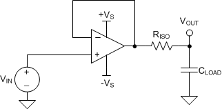 Figure 41. Unity-Gain Buffer With RISO Stability Compensation
8.2.1 Design Requirements
The design requirements are:
- Supply voltage: 30 V (±15 V)
- Capacitive loads: 100-pF, 1000-pF, 0.01-μF, 0.1-μF, and 1-μF
- Phase margin: 45° and 60°
8.2.2 Detailed Design Procedure
Figure 41 shows a unity-gain buffer driving a capacitive load. Equation 1 shows the transfer function for the circuit in Figure 41. Not shown in Figure 41 is the open-loop output resistance of the operational amplifier, RO.

The transfer function in Equation 1 has a pole and a zero. The frequency of the pole (fp) is determined by (RO + RISO) and CLOAD. RISO and CLOAD determine the frequency of the zero (fz). A stable system is obtained by selecting RISO, so the rate of closure (ROC) between the open-loop gain (AOL) and 1/β is 20 dB / decade. Figure 42 depicts the concept. The 1/β curve for a unity-gain buffer is 0 dB.
 Figure 42. Unity-Gain Amplifier With RISO Compensation
ROC stability analysis is typically simulated. The validity of the analysis depends on multiple factors, especially the accurate modeling of R O . In addition to simulating the ROC, a robust stability analysis includes a measurement of overshoot percentage and ac gain peaking of the circuit using a function generator, oscilloscope, and gain and phase analyzer. Phase margin is then calculated from these measurements. Table 6 shows the overshoot percentage and ac gain peaking that correspond to 45° and 60° phase margins. For more details on this design and other alternative devices that can be used in place of the OPAx170-Q1 family, see Capacitive Load Drive Solution Using an Isolation Resistor.
Table 6. Phase Margin versus Overshoot and AC Gain Peaking
| PHASE MARGIN | OVERSHOOT | AC GAIN PEAKING |
|---|---|---|
| 45° | 23.3% | 2.35 dB |
| 60° | 8.8% | 0.28 dB |
8.2.3 Application Curve
Using the described methodology, the values of RISO that yield phase margins of 45º and 60º for various capacitive loads were determined. Figure 43 shows the results.
 Figure 43. Isolation Resistor Required for Various Capacitive Loads to Achieve a Target Phase Margin
9 Power Supply Recommendations
The OPAx170-Q1 family is specified for operation from 2.7 V to 36 V (±1.35 V to ±18 V); many specifications apply from –40°C to +125°C. Parameters that can exhibit significant variance with regard to operating voltage or temperature are presented in Table 4.
CAUTION
Supply voltages larger than 40 V can permanently damage the device; see the Absolute Maximum Ratings table.
Place 0.1-μF bypass capacitors close to the power-supply pins to reduce errors coupling in from noisy or high-impedance power supplies. For more detailed information on bypass capacitor placement, see the Layout section.


