SBOSA11E March 2020 – December 2023 OPA206 , OPA2206 , OPA4206
PRODUCTION DATA
- 1
- 1 Features
- 2 Applications
- 3 Description
- 4 Pin Configuration and Functions
- 5 Specifications
- 6 Parameter Measurement Information
- 7 Detailed Description
- 8 Application and Implementation
- 9 Device and Documentation Support
- 10Revision History
- 11Mechanical, Packaging, and Orderable Information
Package Options
Refer to the PDF data sheet for device specific package drawings
Mechanical Data (Package|Pins)
- D|14
- PW|14
Thermal pad, mechanical data (Package|Pins)
Orderable Information
3 Description
The OPA206, OPA2206, and OPA4206 (OPAx206) are the next generation of the industry-standard OPAx277 family with the added feature of input overvoltage protection. These precision, bipolar, e‑trim™ op amps with super-beta inputs use TI’s proprietary trimming technology to achieve an input offset voltage of ±4 μV (typical) and an input offset voltage drift of ±0.08 μV/°C (typical). The input overvoltage protection activates when the input signal exceeds the supply range and protects up to 40 V beyond either supply. This feature eliminates the need for external circuitry to prevent amplifier damage, thereby reducing size and costs.
The OPAx206 provide a speed-to-power ratio of 3.6 MHz for a mere 220 μA (typical). These devices also achieve a low voltage noise density of only 8 nV/√Hz at 1 kHz. The super-beta inputs of the OPAx206 have a very low input bias current of 100 pA (typical) and a current noise density of 110 fA/√Hz.
The high performance of the OPAx206 make these devices an excellent choice for systems requiring high precision and low power consumption, such as high-density analog input modules in programmable logic controllers, field and portable instrumentation systems, and source measurement units. The OPA205 and OPA2205 are related devices with the same op amp core without the input protection, but with improved broadband noise (7.2 nV/√Hz).
| PART NUMBER | CHANNELS | PACKAGE(1) |
|---|---|---|
| OPA206 | Single | D (SOIC, 8) |
| OPA2206 | Dual | D (SOIC, 8) |
| DGK (VSSOP, 8) | ||
| OPA4206 | Quad | D (SOIC, 14) |
| PW (TSSOP, 14) |
 OPAx206
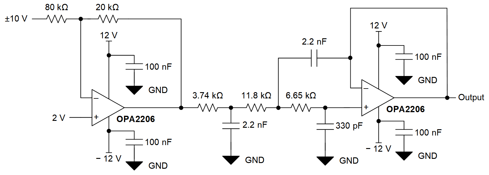
Typical Application