SBOS771B December   2016  – November 2024 OPA4277-SP

PRODUCTION DATA  

  1.   1
  2. Features
  3. Applications
  4. Description
  5. Pin Configuration and Functions
    1. 4.1 Bare Die Information
  6. Specifications
    1. 5.1 Absolute Maximum Ratings
    2. 5.2 ESD Ratings
    3. 5.3 Recommended Operating Conditions
    4. 5.4 Thermal Information
    5. 5.5 Electrical Characteristics
    6. 5.6 Typical Characteristics
  7. Detailed Description
    1. 6.1 Overview
    2. 6.2 Functional Block Diagram
    3. 6.3 Feature Description
      1. 6.3.1 Input Protection
      2. 6.3.2 Input Bias Current Cancellation
    4. 6.4 Device Functional Modes
  8. Application and Implementation
    1. 7.1 Application Information
    2. 7.2 Typical Application
      1. 7.2.1 Design Requirements
      2. 7.2.2 Detailed Design Procedure
      3. 7.2.3 Application Curve
    3. 7.3 Power Supply Recommendations
    4. 7.4 Layout
      1. 7.4.1 Layout Guidelines
      2. 7.4.2 Layout Example
  9. Device and Documentation Support
    1. 8.1 Receiving Notification of Documentation Updates
    2. 8.2 Support Resources
    3. 8.3 Trademarks
    4. 8.4 Electrostatic Discharge Caution
    5. 8.5 Glossary
  10. Revision History
  11. 10Mechanical, Packaging, and Orderable Information

Package Options

Refer to the PDF data sheet for device specific package drawings

Mechanical Data (Package|Pins)
  • JDJ|28
  • HFR|14
  • KGD|0
Thermal pad, mechanical data (Package|Pins)
Orderable Information

Typical Characteristics

at TJ = 25°C, VS = ±15 V, RL = 2 kΩ, and pre-irradiated (unless otherwise noted)
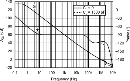
OPA4277-SP Open-Loop Gain and Phase
                        vs Frequency
 
Figure 5-1 Open-Loop Gain and Phase vs Frequency
OPA4277-SP Input
                        Noise and Current Noise Spectral Density vs Frequency
 
Figure 5-3 Input Noise and Current Noise Spectral Density vs Frequency
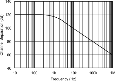
OPA4277-SP Channel Separation vs Frequency
G = 1, measured channel A to D or B to C.
Other combinations yield similar or improved rejection.
Figure 5-5 Channel Separation vs Frequency
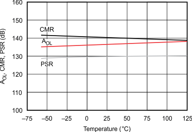
OPA4277-SP AOL, CMR, PSR vs Temperature
 
Figure 5-7 AOL, CMR, PSR vs Temperature
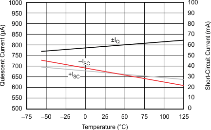
OPA4277-SP Quiescent Current and Short-Circuit Current vs Temperature


Figure 5-9 Quiescent Current and Short-Circuit Current vs Temperature
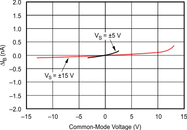
OPA4277-SP Change in Input Bias Current vs Common-Mode Voltage
Curve shows normalized change in bias current with respect to VCM = 0 V. Typical IB can range from –0.5 nA to 0.5 nA at VCM = 0 V.
Figure 5-11 Change in Input Bias Current vs Common-Mode Voltage
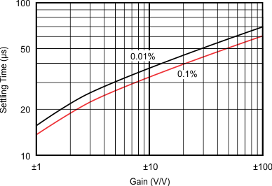
OPA4277-SP Settling Time vs Closed-Loop Gain
10-V stepCL = 1500 pF
Figure 5-13 Settling Time vs Closed-Loop Gain
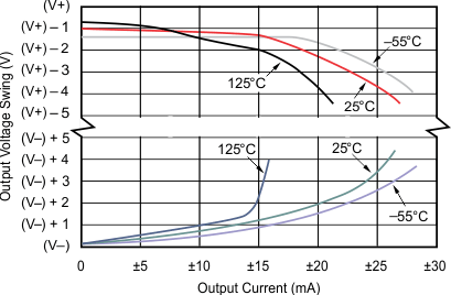
OPA4277-SP Output Voltage Swing vs Output Current
 
Figure 5-15 Output Voltage Swing vs Output Current
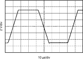
OPA4277-SP Large-Signal Step Response
G = 1CL = 1500 pFVS = ±15 V
Figure 5-17 Large-Signal Step Response
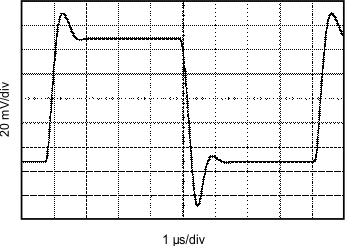
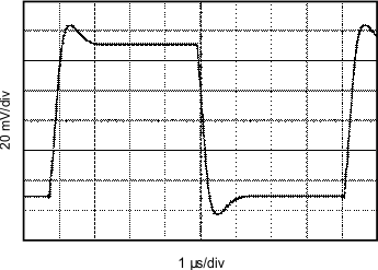
OPA4277-SP Small-Signal Step Response
G = 1 CL = 1500 pF VS = ±15 V
Figure 5-19 Small-Signal Step Response
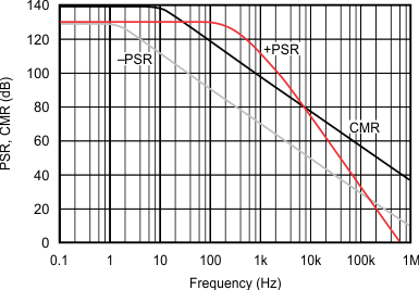
OPA4277-SP Power
                        Supply and Common-Mode Rejection vs Frequency
 
Figure 5-2 Power Supply and Common-Mode Rejection vs Frequency
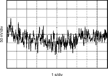
OPA4277-SP Input
                        Noise Voltage vs Time
Noise signal is bandwidth limited to lie between 0.1 Hz and 10 Hz
Figure 5-4 Input Noise Voltage vs Time
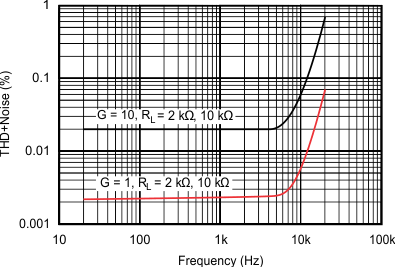
OPA4277-SP Total Harmonic Distortion + Noise vs Frequency
VOUT = 3.5 Vrms
 
Figure 5-6 Total Harmonic Distortion + Noise vs Frequency
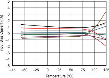
OPA4277-SP Input Bias Current vs Temperature
Curves represent typical production units.
Figure 5-8 Input Bias Current vs Temperature
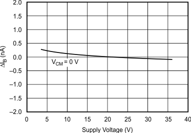
OPA4277-SP Change in Input Bias Current vs Power Supply Voltage
Curve shows normalized change in bias current with respect to VS = ±10 V (+20 V). Typical IB can range from –0.5 nA to 0.5 nA at VS = ±10 V.
Figure 5-10 Change in Input Bias Current vs Power Supply Voltage
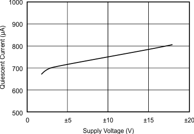
OPA4277-SP Quiescent Current vs Supply Voltage
Per amplifier
 
Figure 5-12 Quiescent Current vs Supply Voltage
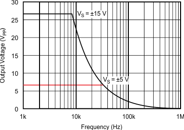
OPA4277-SP Maximum Output Voltage vs Frequency
 
Figure 5-14 Maximum Output Voltage vs Frequency
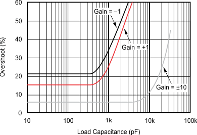
OPA4277-SP Small-Signal Overshoot vs Load Capacitance
 
Figure 5-16 Small-Signal Overshoot vs Load Capacitance
OPA4277-SP Small-Signal Step Response
G = 1CL = 0 pFVS = ±15 V
Figure 5-18 Small-Signal Step Response