SBOS233G March   2002  – April 2018 OPA2354 , OPA354 , OPA4354

PRODUCTION DATA.  

  1. Features
  2. Applications
  3. Description
    1.     Device Images
      1.      Simplified Schematic
  4. Revision History
  5. Device Comparison Table
  6. Pin Configuration and Functions
    1.     Pin Functions: OPA354
    2.     Pin Functions: OPA2354
    3.     Pin Functions: OPA4354
  7. Specifications
    1. 7.1 Absolute Maximum Ratings
    2. 7.2 ESD Ratings
    3. 7.3 Recommended Operating Conditions
    4. 7.4 Thermal Information: OPA354
    5. 7.5 Thermal Information: OPA2354
    6. 7.6 Thermal Information: OPA4354
    7. 7.7 Electrical Characteristics: VS = 2.7 V to 5.5 V (Single-Supply)
    8. 7.8 Typical Characteristics
  8. Detailed Description
    1. 8.1 Overview
    2. 8.2 Functional Block Diagram
    3. 8.3 Feature Description
      1. 8.3.1 Operating Voltage
      2. 8.3.2 Rail-to-Rail Input
      3. 8.3.3 Rail-to-Rail Output
      4. 8.3.4 Output Drive
      5. 8.3.5 Video
      6. 8.3.6 Driving Analog-to-Digital converters
      7. 8.3.7 Capacitive Load and Stability
      8. 8.3.8 Wideband Transimpedance Amplifier
    4. 8.4 Device Functional Modes
  9. Application and Implementation
    1. 9.1 Application Information
    2. 9.2 Typical Application
      1. 9.2.1 Design Requirements
      2. 9.2.2 Detailed Design Procedure
        1. 9.2.2.1 Optimizing the Transimpedance Circuit
      3. 9.2.3 Application Curve
  10. 10Power Supply Recommendations
  11. 11Layout
    1. 11.1 Layout Guidelines
    2. 11.2 Layout Example
    3. 11.3 Power Dissipation
    4. 11.4 PowerPAD Thermally-Enhanced Package
    5. 11.5 PowerPAD Assembly Process
  12. 12Device and Documentation Support
    1. 12.1 Documentation Support
    2. 12.2 Related Links
    3. 12.3 Receiving Notification of Documentation Updates
    4. 12.4 Community Resources
    5. 12.5 Trademarks
    6. 12.6 Electrostatic Discharge Caution
    7. 12.7 Glossary
  13. 13Mechanical, Packaging, and Orderable Information

Package Options

Mechanical Data (Package|Pins)
Thermal pad, mechanical data (Package|Pins)
Orderable Information

Typical Characteristics

at TA = 25°C, VS = 5 V, G = +1, RF = 0 Ω, RL = 1 kΩ, and connected to VS / 2, (unless otherwise noted)
OPA354 OPA2354 OPA4354 tc_noninverting_sm-signal_fqcy_resp_bos233.gif
Figure 1. Noninverting Small-Signal Frequency Response
OPA354 OPA2354 OPA4354 tc_noninverting_sm-signal_step_resp_bos233.gif
Figure 3. Noninverting Small-Signal Step Response
OPA354 OPA2354 OPA4354 tc_gain_flatness_bos233.gif
Figure 5. 0.1-dB Gain Flatness
OPA354 OPA2354 OPA4354 tc_harmonic_distortion_noninverting_gain_bos233.gif
Figure 7. Harmonic Distortion vs Noninverting Gain
OPA354 OPA2354 OPA4354 tc_harmonic_distortion_frequency_bos233.gif
Figure 9. Harmonic Distortion vs Frequency
OPA354 OPA2354 OPA4354 tc_voltage_current_noise_spec_density_fqcy_bos233.gif
Figure 11. Input Voltage and Current Noise Spectral Density vs Frequency
OPA354 OPA2354 OPA4354 tc_frequency_resp_cloads_bos233.gif
Figure 13. Frequency Response for Various CL Values
OPA354 OPA2354 OPA4354 tc_frequency_resp_cload_bos233.gif
Figure 15. Frequency Response vs Capacitive Load
OPA354 OPA2354 OPA4354 tc_open_loop_gain_phase_bos233.gif
Figure 17. Open-Loop Gain and Phase
OPA354 OPA2354 OPA4354 tc_ibias_temp_bos233.gif
Figure 19. Input Bias Current vs Temperature
OPA354 OPA2354 OPA4354 tc_isupply_temp_bos233.gif
Figure 21. Supply Current vs Temperature
OPA354 OPA2354 OPA4354 tc_closed_loop_output_imped_fqcy_bos233.gif
Figure 23. Closed-Loop Output Impedance vs Frequency
OPA354 OPA2354 OPA4354 tc_output_settling_time_bos233.gif
Figure 25. Output Settling Time to 0.1%
OPA354 OPA2354 OPA4354 tc_voffset_prod_distribution_bos233.gif
Figure 27. Offset Voltage Production Distribution
OPA354 OPA2354 OPA4354 tc_crosstalk_bos233.gif
Figure 29. Channel-to-Channel Crosstalk
OPA354 OPA2354 OPA4354 tc_inverting_sm-signal_fqcy_resp_bos233.gif
Figure 2. Inverting Small-Signal Frequency Response
OPA354 OPA2354 OPA4354 tc_noninverting_lg-signal_step_resp_bos233.gif
Figure 4. Noninverting Large-Signal Step Response
OPA354 OPA2354 OPA4354 tc_harmonic_distortion_vout_bos233.gif
Figure 6. Harmonic Distortion vs Output Voltage
OPA354 OPA2354 OPA4354 tc_harmonic_distortion_inverting_gain_bos233.gif
Figure 8. Harmonic Distortion vs Inverting Gain
OPA354 OPA2354 OPA4354 tc_harmonic_distortion_rload_bos233.gif
Figure 10. Harmonic Distortion vs Load Resistance
OPA354 OPA2354 OPA4354 tc_frequency_resp_rloads_bos233.gif
Figure 12. Frequency Response for Various RL Values
OPA354 OPA2354 OPA4354 tc_recommended_rs_cload_bos233.gif
Figure 14. Recommended RS vs Capacitive Load
OPA354 OPA2354 OPA4354 tc_cmrr_psrr_fqcy_bos233.gif
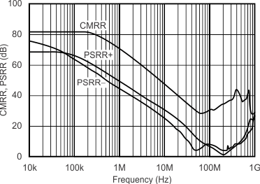
Figure 16. Common-Mode Rejection Ratio and Power-Supply Rejection Ratio vs Frequency
OPA354 OPA2354 OPA4354 tc_differential_gain_phase_bos233.gif
Figure 18. Composite Video Differential Gain and Phase
OPA354 OPA2354 OPA4354 tc_3V_vout_swing_iout_bos233.gif
VS = 3 V
Figure 20. Output Voltage Swing vs Output Current
OPA354 OPA2354 OPA4354 tc_5V_vout_swing_iout_bos233.gif
VS = 5 V
Figure 22. Output Voltage Swing vs Output Current
OPA354 OPA2354 OPA4354 tc_vout_max_fqcy_bos233.gif
Figure 24. Maximum Output Voltage vs Frequency
OPA354 OPA2354 OPA4354 tc_open_loop_gain_temp_bos233.gif
Figure 26. Open-Loop Gain vs Temperature
OPA354 OPA2354 OPA4354 tc_cmrr_psrr_temp_bos233.gif
Figure 28. Common-Mode Rejection Ratio and Power-Supply Rejection Ratio vs Temperature