SBOS803A
December 2018 – December 2019
OPA462
PRODUCTION DATA.
1
Features
2
Applications
3
Description
Device Images
OPA462 Block Diagram
Maximum Output Voltage vs Frequency
4
Revision History
5
Pin Configuration and Functions
Pin Functions
6
Specifications
6.1
Absolute Maximum Ratings
6.2
ESD Ratings
6.3
Recommended Operating Conditions
6.4
Thermal Information
6.5
Electrical Characteristics
6.6
Typical Characteristics: Table of Graphs
6.7
Typical Characteristics
7
Detailed Description
7.1
Overview
7.2
Functional Block Diagram
7.3
Feature Description
7.3.1
Status Flag Pin
7.3.2
Thermal Protection
7.3.3
Current Limit
7.3.4
Enable and Disable
7.4
Device Functional Modes
8
Application and Implementation
8.1
Application Information
8.2
Typical Applications
8.2.1
High DAC Gain Stage for Semiconductor Test Equipment
8.2.1.1
Design Requirements
8.2.1.2
Detailed Design Procedure
8.2.1.3
Application Curve
8.2.2
Improved Howland Current Pump for Bioimpedance Measurements in Multiparameter Patient Monitors
8.2.2.1
Design Requirements
8.2.2.2
Detailed Design Procedure
9
Power Supply Recommendations
10
Layout
10.1
Layout Guidelines
10.1.1
Thermally-Enhanced PowerPAD Package
10.1.2
PowerPAD Integrated Circuit Package Layout Guidelines
10.1.3
Pin Leakage
10.1.4
Thermal Protection
10.1.5
Power Dissipation
10.1.6
Heat Dissipation
10.2
Layout Example
11
Device and Documentation Support
11.1
Device Support
11.1.1
Development Support
11.1.1.1
TINA-TI™ (Free Software Download)
11.1.1.2
TI Precision Designs
11.1.1.3
WEBENCH Filter Designer
11.2
Documentation Support
11.2.1
Related Documentation
11.3
Support Resources
11.4
Trademarks
11.5
Electrostatic Discharge Caution
11.6
Glossary
12
Mechanical, Packaging, and Orderable Information
Package Options
Mechanical Data (Package|Pins)
DDA|8
MPDS092F
Thermal pad, mechanical data (Package|Pins)
DDA|8
PPTD043J
Orderable Information
sbos803a_oa
sbos803a_pm
6.7
Typical Characteristics
at T
A
= 25°C, V
S
= ±90 V, and R
L
= 10 kΩ connected to GND, output enabled (unless otherwise noted)
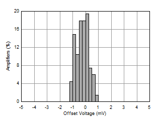
Figure 1.
Offset Voltage Production Distribution at 25°C
Figure 3.
Offset Voltage Distribution at –40°C
Figure 5.
Offset Voltage vs Temperature
Figure 7.
Offset Voltage vs Common-Mode Voltage
(Low V
CM
)
Figure 9.
Offset Voltage vs Power Supply (Low Supply)
Figure 11.
Offset Voltage vs Output Voltage (Low Output)
Figure 13.
CMRR vs Temperature
Figure 15.
PSRR vs Temperature
Figure 17.
EMIRR vs Frequency
Figure 19.
Input Bias Current Production Distribution at 25℃
Figure 21.
IB vs Common-Mode Voltage
Figure 23.
Current Limit Response
Figure 25.
Open-Loop Gain vs Output Voltage
Figure 27.
Open-Loop Output Impedance vs Frequency
Figure 29.
Maximum Output Voltage vs Frequency
Figure 31.
Negative Output Voltage vs Output Current
Figure 33.
Negative Overload Recovery
Figure 35.
Settling Time
G = –1
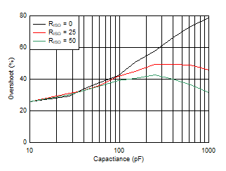
Figure 37.
Small-Signal Overshoot vs Capacitive Load
G = –1
Figure 39.
Small-Signal Step Response
G = –1
Figure 41.
Large-Signal Step Response
Figure 43.
Slew Rate vs Output Step Size
Figure 45.
Slew Rate vs Supply Voltage (Noninverting)
G = 20
Figure 47.
THD+N Ratio vs Frequency
G = 20
Figure 49.
THD+N Ratio vs Output Amplitude
Figure 51.
Input Voltage Noise Spectral Density
Figure 53.
Quiescent Current Production Distribution at 25℃
Figure 55.
Quiescent Current vs Temperature
Figure 57.
Quiescent Current vs Enable Voltage
Figure 59.
Status Flag Current vs Voltage
Figure 2.
Offset Voltage Distribution at 85°C
Figure 4.
Offset Voltage Drift Distribution from –40°C to +85°C
Figure 6.
Offset Voltage Warmup
Figure 8.
Offset Voltage vs Common-Mode Voltage
(High V
CM
)
Figure 10.
Offset Voltage vs Power Supply (High Supply)
Figure 12.
Offset Voltage vs Output Voltage (High Output)
Figure 14.
CMRR vs Frequency
Figure 16.
PSRR vs Frequency
Figure 18.
No Phase Reversal
Figure 20.
IB vs Temperature
Figure 22.
Enable Response
Figure 24.
Open-Loop Gain vs Temperature
Figure 26.
Open-Loop Gain and Phase vs Frequency
Figure 28.
Closed-Loop Gain vs Frequency
Figure 30.
Positive Output Voltage vs Output Current
Figure 32.
Short-Circuit Current vs Temperature
Figure 34.
Positive Overload Recovery
Figure 36.
Phase Margin vs Capacitive Load
G = +1
Figure 38.
Small-Signal Overshoot vs Capacitive Load
G = +1
Figure 40.
Small-Signal Step Response
G = +1
Figure 42.
Large-Signal Step Response
Figure 44.
Slew Rate vs Supply Voltage (Inverting)
G = 10
Figure 46.
THD+N Ratio vs Frequency
G = 10
Figure 48.
THD+N Ratio vs Output Amplitude
Figure 50.
0.1-Hz to 10-Hz Noise
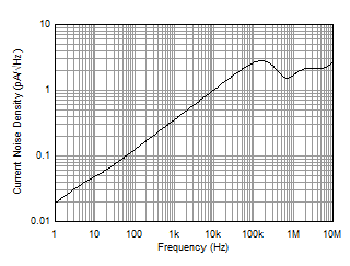
Figure 52.
Current Noise Density
Figure 54.
Quiescent Current vs Supply Voltage
Figure 56.
Status Flag Voltage vs Temperature
Figure 58.
Enable Current vs Enable Voltage