SBOS933I February 2019 – August 2021 OPA2990 , OPA4990 , OPA990
PRODUCTION DATA
- 1 Features
- 2 Applications
- 3 Description
- 4 Revision History
- 5 Pin Configuration and Functions
- 6 Specifications
-
7 Detailed Description
- 7.1 Overview
- 7.2 Functional Block Diagram
- 7.3
Feature Description
- 7.3.1 Input Protection Circuitry
- 7.3.2 EMI Rejection
- 7.3.3 Thermal Protection
- 7.3.4 Capacitive Load and Stability
- 7.3.5 Common-Mode Voltage Range
- 7.3.6 Phase Reversal Protection
- 7.3.7 Electrical Overstress
- 7.3.8 Overload Recovery
- 7.3.9 Typical Specifications and Distributions
- 7.3.10 Packages With an Exposed Thermal Pad
- 7.3.11 Shutdown
- 7.4 Device Functional Modes
- 8 Application and Implementation
- 9 Power Supply Recommendations
- 10Layout
- 11Device and Documentation Support
- 12Mechanical, Packaging, and Orderable Information
Package Options
Mechanical Data (Package|Pins)
Thermal pad, mechanical data (Package|Pins)
Orderable Information
7.3.6 Phase Reversal Protection
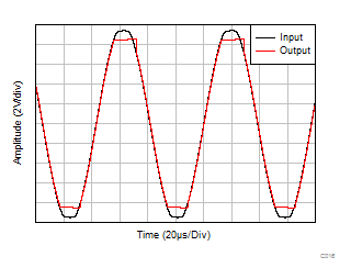
The OPAx990 family has internal phase-reversal protection. Many op amps exhibit a phase reversal when the input is driven beyond its linear common-mode range. This condition is most often encountered in non-inverting circuits when the input is driven beyond the specified common-mode voltage range, causing the output to reverse into the opposite rail. The OPAx990 is a rail-to-rail input op amp; therefore, the common-mode range can extend up to the rails. Input signals beyond the rails do not cause phase reversal; instead, the output limits into the appropriate rail. This performance is shown in Figure 7-9. For more information on phase reversal, see Op Amps With Complementary-Pair Input Stages application note.
 Figure 7-9 No Phase
Reversal