SBOS070D October   1997  – December 2019 OPA548

PRODUCTION DATA.  

  1. Features
  2. Applications
    1.     Simplified Schematic
  3. Description
  4. Revision History
  5. Pin Configuration and Functions
    1.     Pin Functions
  6. Specifications
    1. 6.1 Absolute Maximum Ratings
    2. 6.2 ESD Ratings
    3. 6.3 Recommended Operating Conditions
    4. 6.4 Thermal Information
    5. 6.5 Electrical Characteristics
    6. 6.6 Typical Characteristics
  7. Detailed Description
    1. 7.1 Overview
    2. 7.2 Functional Block Diagram
    3. 7.3 Feature Description
      1. 7.3.1 Adjustable Current Limit
      2. 7.3.2 Enable/Status (E/S) Pin
      3. 7.3.3 Thermal Shutdown Status
    4. 7.4 Device Functional Modes
      1. 7.4.1 Output Disable
  8. Application and Implementation
    1. 8.1 Application Information
    2. 8.2 Typical Applications
      1. 8.2.1 Basic Circuit Connections
        1. 8.2.1.1 Design Requirements
        2. 8.2.1.2 Detailed Design Procedure
          1. 8.2.1.2.1 Power Supply Requirements
          2. 8.2.1.2.2 Gain Setting and Input Configuration
          3. 8.2.1.2.3 Current Limit
          4. 8.2.1.2.4 Safe-Operating-Area
          5. 8.2.1.2.5 Heat Sinking
        3. 8.2.1.3 Application Curve
      2. 8.2.2 Monitoring Single- and Dual-Supplies
        1. 8.2.2.1 Design Requirements
        2. 8.2.2.2 Detailed Design Procedure
          1. 8.2.2.2.1 Output Disable and Thermal Shutdown Status
      3. 8.2.3 Programmable Power Supply
    3. 8.3 System Examples
  9. Power Supply Recommendations
    1. 9.1 Output Stage Compensation
    2. 9.2 Output Protection
  10. 10Layout
    1. 10.1 Layout Guidelines
      1. 10.1.1 Safe Operating Area
      2. 10.1.2 Amplifier Mounting
      3. 10.1.3 Power Dissipation
      4. 10.1.4 Thermal Considerations
      5. 10.1.5 Heat Sinking
        1. 10.1.5.1 Heat Sink Selection Example
    2. 10.2 Layout Example
  11. 11Device and Documentation Support
    1. 11.1 Device Support
      1. 11.1.1 Third-Party Products Disclaimer
    2. 11.2 Documentation Support
      1. 11.2.1 Related Documentation
    3. 11.3 Receiving Notification of Documentation Updates
    4. 11.4 Support Resources
    5. 11.5 Trademarks
    6. 11.6 Electrostatic Discharge Caution
    7. 11.7 Glossary
  12. 12Mechanical, Packaging, and Orderable Information

Package Options

Mechanical Data (Package|Pins)
Thermal pad, mechanical data (Package|Pins)
Orderable Information

Typical Characteristics

at TCASE = 25°C, VS = ±30V, and E/S pin open (unless otherwise noted)
OPA548 typchar1.png
Figure 1. Open-Loop Gain and Phase vs Frequency
OPA548 typchar3.png
Figure 3. Current Limit vs Temperature
OPA548 typchar5.png
Figure 5. Input Bias Current vs Common-Mode Voltage
OPA548 typchar7.png
Figure 7. Common-Mode Rejection vs Frequency
OPA548 typchar9.png
Figure 9. Voltage Noise Density vs Frequency
OPA548 typchar11.png
Figure 11. Gain-Bandwidth Product and Slew Rate vs Temperature
OPA548 typchar13.gif
Figure 13. Output Voltage Swing vs Output Current
OPA548 typchar15.png
Figure 15. Maximum Output Voltage Swing vs Frequency
OPA548 typchar17.png
Figure 17. Offset Voltage Production Distribution
OPA548 typchar19.png
Figure 19. Small-Signal Overshoot vs Load Capacitance
OPA548 typchar21.png
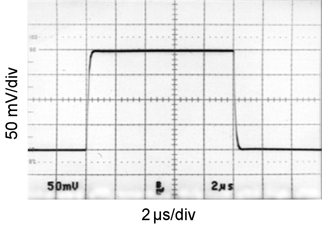
G = 1 CL = 1000 pF
Figure 21. Small-Signal Step Response
OPA548 typchar2.png
Figure 2. Input Bias Current vs Temperature
OPA548 typchar4.png
Figure 4. Current Limit vs Supply Voltage
OPA548 typchar6.png
Figure 6. Quiescent Current vs Temperature
OPA548 typchar8.png
Figure 8. Power-Supply Rejection vs Frequency
OPA548 typchar10.png
Figure 10. Open-loop Gain, Common-Mode Rejection,
and Power-Supply Rejection vs Temperature
OPA548 typchar12.png
Figure 12. Total Harmonic Distortion+Noise vs Frequency
OPA548 typchar14.gif
Figure 14. Output Voltage Swing vs Temperature
OPA548 typchar16.png
Figure 16. Output Leakage Current vs Applied Output Voltage
OPA548 typchar18.png
Figure 18. Offset Voltage Drift Production Distribution
OPA548 typchar20.gif
G = 3 CL = 1000 pF, RL = 8 Ω
Figure 20. Large-Signal Step Response
OPA548 typchar22.png
G = 3 CL = 1000 pF
Figure 22. Small-Signal Step Response