SBOS567A June   2011  – February 2024 OPA564-Q1

PRODUCTION DATA  

  1.   1
  2. Features
  3. Applications
  4. Description
  5. Device Comparison Table
  6. Pin Configuration and Functions
  7. Specifications
    1. 6.1 Absolute Maximum Ratings
    2. 6.2 ESD Ratings
    3. 6.3 Recommended Operating Conditions
    4. 6.4 Thermal Information
    5. 6.5 Electrical Characteristics
    6. 6.6 Typical Characteristics
  8. Detailed Description
    1. 7.1 Overview
    2. 7.2 Functional Block Diagram
    3. 7.3 Feature Description
      1. 7.3.1 Adjustable Current Limit
        1. 7.3.1.1 Setting the Current Limit
      2. 7.3.2 Enable and Shutdown (E/S) Pin
      3. 7.3.3 Input Protection
      4. 7.3.4 Output Shutdown
      5. 7.3.5 Microcontroller Compatibility
      6. 7.3.6 Current Limit Flag
      7. 7.3.7 Thermal Protection
      8. 7.3.8 Junction Temperature Measurement Using TSENSE
    4. 7.4 Device Functional Modes
  9. Application and Implementation
    1. 8.1 Application Information
      1. 8.1.1 Basic Configuration
      2. 8.1.2 Output-Stage Compensation
      3. 8.1.3 Output Protection
      4. 8.1.4 Power Dissipation and Safe Operating Area
    2. 8.2 Typical Applications
      1. 8.2.1 Improved Howland Current Pump
      2. 8.2.2 Programmable Power Supply
      3. 8.2.3 Powerline Communication
      4. 8.2.4 Motor-Drive Circuit
      5. 8.2.5 DC Motor-Speed Controller (Without Tachometer)
      6. 8.2.6 Generating VDIG
      7. 8.2.7 Temperature Measurement
    3. 8.3 Power Supply Recommendations
    4. 8.4 Layout
      1. 8.4.1 Layout Guidelines
        1. 8.4.1.1 Thermally Enhanced PowerPAD™ Integrated Circuit Package
          1. 8.4.1.1.1 Bottom-Side Thermal Pad Assembly Process
  10. Device and Documentation Support
    1. 9.1 Receiving Notification of Documentation Updates
    2. 9.2 Support Resources
    3. 9.3 Trademarks
    4. 9.4 Electrostatic Discharge Caution
    5. 9.5 Glossary
  11. 10Revision History
  12. 11Mechanical, Packaging, and Orderable Information

Package Options

Refer to the PDF data sheet for device specific package drawings

Mechanical Data (Package|Pins)
  • DWP|20
Thermal pad, mechanical data (Package|Pins)
Orderable Information

Powerline Communication

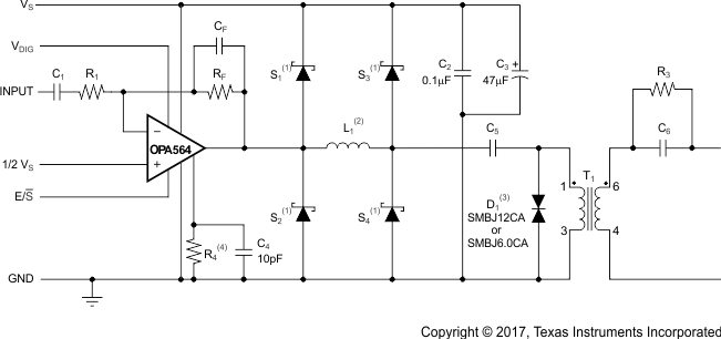
Powerline-communication (PLC) applications require some form of signal transmission over an existing ac power line. A common technique used to couple these modulated signals to the line is through a signal transformer. A power amplifier is often needed to provide adequate levels of current and voltage to drive the varying loads that exist on modern powerlines. Figure 8-8 shows one such application. The OPA564-Q1 is used to drive signals used in frequency modulation schemes such as frequency-shift keying (FSK) or orthogonal frequency-division multiplexing (OFDM) to transmit digital information over the powerline. The power output capabilities of the OPA564-Q1 are needed to drive the current requirements of the transformer that is shown in the figure, coupled to the ac power line via a coupling capacitor. Circuit protection is often required to prevent excessive line voltages or current surges from damaging the active circuitry in the power amplifier and application circuitry.
GUID-55FD2A1D-D1B6-41DA-9326-63ECCC8FCC11-low.gif
1. S1, S2, S3, and S4 are Schottky diodes. S1 and S2 are B350 or equivalent. S3 and S4 are BAV99T or equivalent.
2. Ensure that L1 is small enough so that L1 does not interfere with the bandwidth of interest, but large enough to suppress transients that can damage the OPA564-Q1.
3. D1 is a transient suppression diode. For 24V supplies, use SMBJ12CA. For 12V supplies, use SMBJ6.0CA. Ensure that the voltage rating of the transient voltage suppressor is half the supply rating or less.
4. The minimum recommended value for R4 is 7.5kΩ.
Figure 8-8 Powerline Communication Line Coupling

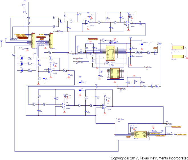
Figure 8-9 illustrates a detailed powerline communication circuit.
GUID-B74C1BAD-5C3F-407C-B127-B2E69CE1B72C-low.gif Figure 8-9 Detailed Powerline Communication Circuit