SBOSA38A February   2021  – April 2021 OPA2607-Q1 , OPA607-Q1

PRODUCTION DATA  

  1. Features
  2. Applications
  3. Description
  4. Revision History
  5. Device Comparison
  6. Pin Configuration and Functions
  7. Specifications
    1. 7.1 Absolute Maximum Ratings
    2. 7.2 ESD Ratings
    3. 7.3 Recommended Operating Conditions
    4. 7.4 Thermal Information
    5. 7.5 Electrical Characteristics
    6. 7.6 Typical Characteristics
  8. Detailed Description
    1. 8.1 Overview
    2. 8.2 Functional Block Diagram
    3. 8.3 Feature Description
      1. 8.3.1 Operating Voltage
      2. 8.3.2 Rail-to-Rail Output and Driving Capacitive Loads
      3. 8.3.3 Input and ESD Protection
      4. 8.3.4 Decompensated Architecture with Wide Gain-Bandwidth Product
    4. 8.4 Device Functional Modes
      1. 8.4.1 Normal Operating Mode
  9. Application and Implementation
    1. 9.1 Application Information
    2. 9.2 Typical Applications
      1. 9.2.1 100-kΩ Gain Transimpedance Design
        1. 9.2.1.1 Design Requirements
        2. 9.2.1.2 Detailed Design Procedure
        3. 9.2.1.3 Application Curves
      2. 9.2.2 Noninverting Gain of 3 V/V
      3. 9.2.3 High-Input Impedance (Hi-Z), High-Gain Signal Front-End
        1. 9.2.3.1 Design Requirements
        2. 9.2.3.2 Detailed Design Procedure
        3. 9.2.3.3 Application Curves
      4. 9.2.4 Low-Cost, Low Side, High-Speed Current Sensing
        1. 9.2.4.1 Design Requirements
        2. 9.2.4.2 Detailed Design Procedure
        3. 9.2.4.3 Application Curves
  10. 10Power Supply Recommendations
  11. 11Layout
    1. 11.1 Layout Guidelines
    2. 11.2 Layout Examples
  12. 12Device and Documentation Support
    1. 12.1 Device Support
      1. 12.1.1 Development Support
    2. 12.2 Documentation Support
      1. 12.2.1 Related Documentation
    3. 12.3 Receiving Notification of Documentation Updates
    4. 12.4 Support Resources
    5. 12.5 Trademarks
    6. 12.6 Electrostatic Discharge Caution
    7. 12.7 Glossary
  13. 13Mechanical, Packaging, and Orderable Information

Package Options

Mechanical Data (Package|Pins)
Thermal pad, mechanical data (Package|Pins)
Orderable Information

100-kΩ Gain Transimpedance Design

The high GBW and low input voltage and current noise for the OPAx607-Q1 devices make it an excellent wideband transimpedance amplifier for moderate to high transimpedance gains.
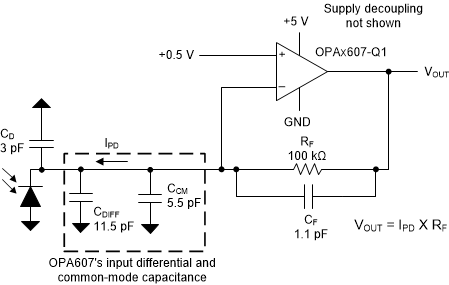
GUID-83A7F321-79DF-422D-B812-6DF14BE5BA3D-low.gifFigure 9-1 Wideband, High-Sensitivity, Transimpedance Amplifier