SBOS981J October 2019 – April 2021 OPA2607 , OPA607
PRODUCTION DATA
- 1 Features
- 2 Applications
- 3 Description
- 4 Revision History
- 5 Device Comparison
- 6 Pin Configuration and Functions
- 7 Specifications
- 8 Detailed Description
- 9 Application and Implementation
- 10Power Supply Recommendations
- 11Layout
- 12Device and Documentation Support
- 13Mechanical, Packaging, and Orderable Information
Package Options
Mechanical Data (Package|Pins)
Thermal pad, mechanical data (Package|Pins)
Orderable Information
6 Pin Configuration and Functions
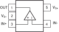
 Figure 6-1 DBV Package
5-Pin SOT-23
Top View
 Figure 6-2 DCK Package
6-Pin SC70
Top View
Pin
Functions – Single Channel
| PIN | I/O | DESCRIPTION | ||
|---|---|---|---|---|
| NAME | DBV | DCK | ||
| IN– | 4 | 3 | I | Inverting input |
| IN+ | 3 | 1 | I | Non inverting input |
| OUT | 1 | 4 | O | Output |
| PD | — | 5 | I | Power down (can be left floating) |
| VS– | 2 | 2 | — | Negative supply or ground (for single-supply operation) |
| VS+ | 5 | 6 | — | Positive supply |
 Figure 6-3 OPA2607 D, DGK Package
 8-Pin SOIC, VSSOP
Top View
 Figure 6-4 OPA2607 RUG Package
 10-Pin X2QFN
Top View
Pin
Functions – Dual Channel
| PIN | I/O | DESCRIPTION | ||
|---|---|---|---|---|
| NAME | D, DGK | RUG | ||
| IN1– | 2 | 2 | I | Inverting input, channel 1 |
| IN1+ | 3 | 3 | I | Noninverting input, channel 1 |
| IN2– | 6 | 8 | I | Inverting input, channel 2 |
| IN2+ | 5 | 7 | I | Noninverting input, channel 2 |
| OUT1 | 1 | 1 | O | Output, channel 1 |
| OUT2 | 7 | 9 | O | Output, channel 2 |
| VS– | 4 | 5 | — | Negative (lowest) supply or ground (for single-supply operation) |
| VS+ | 8 | 10 | — | Positive (highest) supply |
| PD1 | — | 4 | I | Low = amplifier 1 disabled, high = amplifier 1 enabled; see the Power Down Mode section for more information. |
| PD2 | — | 6 | I | Low = amplifier 2 disabled, high = amplifier 2 enabled; see the Power Down Mode section for more information. |