SBOS196I December 2001 – February 2024 OPA656
PRODUCTION DATA
- 1
- 1 Features
- 2 Applications
- 3 Description
- 4 Device Comparison Table
- 5 Pin Configuration and Functions
- 6 Specifications
- 7 Detailed Description
- 8 Application and Implementation
- 9 Device and Documentation Support
- 10Revision History
- 11Mechanical, Packaging, and Orderable Information
Package Options
Refer to the PDF data sheet for device specific package drawings
Mechanical Data (Package|Pins)
- D|8
- DBV|5
Thermal pad, mechanical data (Package|Pins)
Orderable Information
5 Pin Configuration and Functions
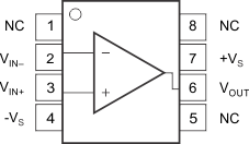
 Figure 5-1 D Package, 8-Pin SOIC
Surface-Mount (Top View)
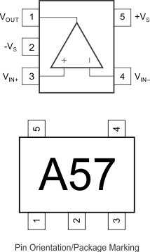
 Figure 5-2 DBV Package, 5-Pin SOT-23
(Top View)
Figure 5-2 DBV Package, 5-Pin SOT-23
(Top View)Table 5-1 Pin Functions
| PIN | TYPE | DESCRIPTION | ||
|---|---|---|---|---|
| NAME | NO. | |||
| D (SOIC) |
DBV (SOT-23) | |||
| NC | 1, 5, 8 | — | — | No internal connection |
| VIN– | 2 | 4 | Input | Inverting input |
| VIN+ | 3 | 3 | Input | Noninverting input |
| –VS | 4 | 2 | Power | Negative power supply |
| +VS | 7 | 5 | Power | Positive power supply |
| VOUT | 6 | 1 | Output | Output of amplifier |