SBOS197F December   2001  – August 2015 OPA657

PRODUCTION DATA.  

  1. Features
  2. Applications
  3. Description
  4. Revision History
  5. Related Operational Amplifier Products
  6. Pin Configuration and Functions
  7. Specifications
    1. 7.1 Absolute Maximum Ratings
    2. 7.2 ESD Ratings
    3. 7.3 Recommended Operating Conditions
    4. 7.4 Thermal Information
    5. 7.5 Electrical Characteristics: VS = ±5 V
    6. 7.6 Electrical Characteristics: VS - ±5 V, High-Grade DC Specifications
    7. 7.7 Typical Characteristics: VS = ±5 V
  8. Detailed Description
    1. 8.1 Overview
    2. 8.2 Feature Description
      1. 8.2.1 Input and ESD Protection
    3. 8.3 Device Functional Modes
      1. 8.3.1 Split-Supply Operation (±4-V to ±6-V)
      2. 8.3.2 Single-Supply Operation (8-V to 12-V)
  9. Application and Implementation
    1. 9.1 Application Information
      1. 9.1.1 Wideband, Noninverting Operation
      2. 9.1.2 Wideband, Inverting Gain Operation
      3. 9.1.3 Low-Gain Compensation
      4. 9.1.4 Operating Suggestions
        1. 9.1.4.1 Setting Resistor Values to Minimize Noise
        2. 9.1.4.2 Frequency Response Control
        3. 9.1.4.3 Driving Capacitive Loads
        4. 9.1.4.4 Distortion Performance
        5. 9.1.4.5 DC Accuracy and Offset Control
    2. 9.2 Typical Application
      1. 9.2.1 Design Requirements
      2. 9.2.2 Detailed Design Procedure
      3. 9.2.3 Application Curves
  10. 10Power Supply Recommendations
  11. 11Layout
    1. 11.1 Layout Guidelines
      1. 11.1.1 Demonstration Fixtures
    2. 11.2 Layout Example
    3. 11.3 Thermal Considerations
  12. 12Device and Documentation Support
    1. 12.1 Community Resources
    2. 12.2 Trademarks
    3. 12.3 Electrostatic Discharge Caution
    4. 12.4 Glossary
  13. 13Mechanical, Packaging, and Orderable Information

Package Options

Mechanical Data (Package|Pins)
Thermal pad, mechanical data (Package|Pins)
Orderable Information

6 Pin Configuration and Functions

D Package
8-Pin SOIC Surface-Mount
Top View
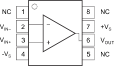
OPA657 po_soic_bos197.gif
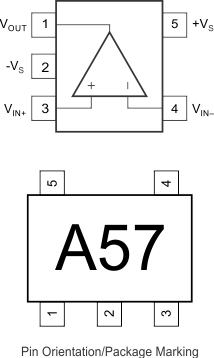
DBV Package
5-Pin SOT-23
Top View
OPA657 po_sot_bos197.gif

Pin Functions

PIN I/O DESCRIPTION
NAME SOIC SOT-23
NC 1 No Connection
5
8
VIN– 2 4 I Inverting Input
VIN+ 3 3 I Noninverting Input
–VS 4 2 POW Negative Power Supply
VOUT 6 1 O Output of amplifier
+VS 7 5 POW Positive Power Supply