SBOS342C December 2008 – November 2015 OPA659
PRODUCTION DATA.
- 1 Features
- 2 Applications
- 3 Description
- 4 Revision History
- 5 Related Operational Amplifier Products
- 6 Pin Configuration and Functions
- 7 Specifications
- 8 Detailed Description
- 9 Application Information
- 10Power Supply Recommendations
- 11Layout
- 12Device and Documentation Support
- 13Mechanical, Packaging, and Orderable Information
Package Options
Mechanical Data (Package|Pins)
Thermal pad, mechanical data (Package|Pins)
- DRB|8
Orderable Information
7 Specifications
7.1 Absolute Maximum Ratings
Over operating free-air temperature range (unless otherwise noted).| MIN | MAX | UNIT | ||
|---|---|---|---|---|
| Power Supply Voltage VS+ to VS– | ±6.5 | V | ||
| Input Voltage | ±VS | V | ||
| Input Current | 100 | mA | ||
| Output Current | 100 | mA | ||
| Continuous Power Dissipation | See Thermal Information | |||
| Operating Free Air Temperature, TA | –40 | 85 | °C | |
| Maximum Junction Temperature, TJ | 150 | °C | ||
| Maximum Junction Temperature, TJ (continuous operation for long term reliability) | 125 | °C | ||
| Storage Temperature, Tstg | –65 | 150 | °C | |
7.2 ESD Ratings
| VALUE | UNIT | |||
|---|---|---|---|---|
| V(ESD) | Electrostatic discharge | Human-body model (HBM), per ANSI/ESDA/JEDEC JS-001(1) | ±4000 | V |
| Charged-device model (CDM), per JEDEC specification JESD22-C101(2) | ±1000 | |||
| Machine model (MM) | ±200 | |||
(1) JEDEC document JEP155 states that 500-V HBM allows safe manufacturing with a standard ESD control process.
(2) JEDEC document JEP157 states that 250-V CDM allows safe manufacturing with a standard ESD control process.
7.3 Recommended Operating Conditions
over operating free-air temperature range (unless otherwise noted)| MIN | NOM | MAX | UNIT | ||
|---|---|---|---|---|---|
| VS | Total supply voltage | 7 | 12 | 13 | V |
| TA | Ambient temperature | –40 | 25 | 85 | °C |
7.4 Thermal Information
| THERMAL METRIC(1) | OPA659 | UNIT | ||
|---|---|---|---|---|
| DRB (VSON) | DRV (SOT23) | |||
| 8 PINS | 5 PINS | |||
| RθJA | Junction-to-ambient thermal resistance | 56.3 | 209 | °C/W |
| RθJC(top) | Junction-to-case (top) thermal resistance | 63.7 | 124 | °C/W |
| RθJB | Junction-to-board thermal resistance | 31.9 | 38.1 | °C/W |
| ψJT | Junction-to-top characterization parameter | 3.2 | 15 | °C/W |
| ψJB | Junction-to-board characterization parameter | 32.1 | 37.2 | °C/W |
| RθJC(bot) | Junction-to-case (bottom) thermal resistance | 15.3 | — | °C/W |
(1) For more information about traditional and new thermal metrics, see the Semiconductor and IC Package Thermal Metrics application report, SPRA953.
7.5 Electrical Characteristics
At RF = 0 Ω, G = 1 V/V, and RL = 100 Ω, TA = 25°C, VS = ±6 V unless otherwise noted.| PARAMETER | TEST CONDITIONS | TEST LEVEL(1) | MIN | TYP | MAX | UNIT | |||
|---|---|---|---|---|---|---|---|---|---|
| AC PERFORMANCE | |||||||||
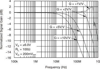
| Small-Signal Bandwidth | VO = 200 mVPP, G = 1 V/V | C | 650 | MHz | |||||
| VO = 200 mVPP, G = 2 V/V | C | 335 | MHz | ||||||
| VO = 200 mVPP, G = 5 V/V | C | 75 | MHz | ||||||
| VO = 200 mVPP, G = 10 V/V | C | 35 | MHz | ||||||
| Gain Bandwidth Product | G > 10 V/V | C | 350 | MHz | |||||
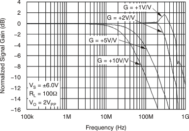
| Bandwidth for 0.1dB Flatness | G = 2 V/V, VO = 2VPP | C | 55 | MHz | |||||
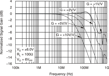
| Large-Signal Bandwidth | VO = 2 VPP, G = 1 V/V | B | 575 | MHz | |||||
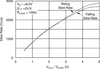
| Slew Rate | VO = 4-V Step, G = 1 V/V | B | 2550 | V/μs | |||||
| Rise and Fall Time | VO = 4-V Step, G = 1 V/V | C | 1.3 | ns | |||||
| Settling Time to 1% | VO = 4-V Step, G = 1 V/V | C | 8 | ns | |||||
| Pulse Response Overshoot | VO = 4-V Step, G = 1 V/V | C | 12% | ||||||
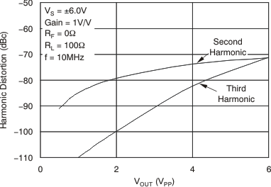
| Harmonic Distortion, 2nd harmonic | VO = 2 VPP, G = 1 V/V, f = 10 MHz | C | –79 | dBc | |||||
| Harmonic Distortion, 3rd harmonic | VO = 2 VPP, G = 1 V/V, f = 10 MHz | C | –100 | dBc | |||||
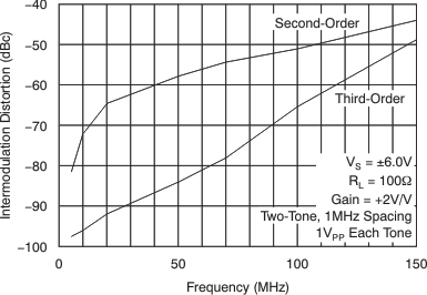
| Intermodulation Distortion, 2nd intermodulation | VO= 2 VPP Envelope (each tone 1 VPP), G = 2 V/V, f1 = 10 MHz, f2 = 11 MHz |
C | –72 | dBc | |||||
| Intermodulation Distortion, 3rd intermodulation | VO= 2 VPP Envelope (each tone 1 VPP), G = 2 V/V, f1 = 10 MHz, f2 = 11 MHz |
C | –96 | dBc | |||||
| Input Voltage Noise | f > 100 kHz | C | 8.9 | nV/√Hz | |||||
| Input Current Noise | f < 10 MHz | C | 1.8 | fA/√Hz | |||||
| DC PERFORMANCE | |||||||||
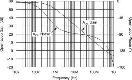
| Open-Loop Voltage Gain (AOL) | TA = 25°C, VCM = 0 V, RL = 100 Ω | A | 52 | 58 | dB | ||||
| TA = –40°C to 85°C, VCM = 0 V, RL = 100 Ω | B | 49 | 55 | dB | |||||
| Input Offset Voltage | TA = 25°C, VCM = 0 V | A | ±1 | ±5 | mV | ||||
| TA = –40°C to 85°C, VCM = 0 V DRB package | DRB package | B | ±1.5 | ±7.6 | mV | ||||
| DBV package | B | ±1.5 | ±8.9 | mV | |||||
| Average input-offset voltage drift(2) | TA = –40°C to 85°C, VCM = 0 V | DRB package | B | ±10 | ±40 | μV/°C | |||
| DBV package | B | ±10 | ±60 | μV/°C | |||||
| Input Bias Current | TA = 25°C, VCM = 0 V | A | ±10 | ±50 | pA | ||||
| TA = 0°C to 70°C, VCM = 0 V | B | ±240 | ±1200 | pA | |||||
| TA = –40°C to 85°C, VCM = 0 V | B | ±640 | ±3200 | pA | |||||
| Average input bias current drift | TA = 0°C to 70°C, VCM = 0 V | B | ±5 | ±26 | pA/°C | ||||
| TA = –40°C to 85°C, VCM = 0 V | B | ±7 | ±34 | pA/°C | |||||
| Input Offset Current | TA = 25°C, VCM = 0 V | A | ±5 | ±25 | pA | ||||
| TA = 0°C to 70°C, VCM = 0 V | B | ±120 | ±600 | pA | |||||
| TA = –40°C to 85°C, VCM = 0 V | B | ±320 | ±1600 | pA | |||||
| INPUT | |||||||||
| Common-Mode Input Range(3) | TA = 25°C | A | ±3 | ±3.5 | V | ||||
| TA = –40°C to 85°C | B | ±2.87 | ±3.37 | V | |||||
| Common-Mode Rejection Ratio | TA = 25°C, VCM = ±0.5 V | A | 68 | 70 | dB | ||||
| TA = –40°C to 85°C, VCM = ±0.5 V | B | 64 | 66 | dB | |||||
| Input Impedance | |||||||||
| Input impedance, differential | C | 1012 ∥ 1 | Ω ∥ pF | ||||||
| Input impedance, common-mode | C | 1012 ∥ 2.5 | Ω ∥ pF | ||||||
| OUTPUT | |||||||||
| Output Voltage Swing | TA = 25°C, | No Load | A | ±4.6 | ±4.8 | V | |||
| RL = 100 Ω | A | ±3.8 | ±4 | V | |||||
| TA = –40°C to 85°C | No Load | B | ±4.45 | ±4.65 | V | ||||
| RL = 100 Ω | B | ±3.65 | ±3.85 | V | |||||
| Output Current, Sourcing, Sinking | TA = 25°C | A | ±60 | ±70 | mA | ||||
| TA = –40°C to 85°C | B | ±56 | ±65 | mA | |||||
| Closed-Loop Output Impedance | G = 1 V/V, f = 100 kHz | C | 0.04 | Ω | |||||
| POWER SUPPLY | |||||||||
| Operating Voltage | B | ±3.5 | ±6 | ±6.5 | V | ||||
| Quiescent Current | TA = 25°C | A | 30.5 | 32 | 33.5 | mA | |||
| TA = –40°C to 85°C | B | 28.3 | 35.7 | mA | |||||
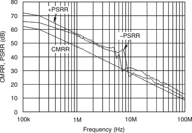
| Power-Supply Rejection Ratio (PSRR) | TA = 25°C, VS = ±5.5 V to ±6.5 V | A | 58 | 62 | dB | ||||
| TA = –40°C to 85°C, VS = ±5.5 V to ±6.5 V | A | 56 | 60 | dB | |||||
(1) Test levels: (A) 100% tested at 25°C. Over temperature limits set by characterization and simulation. (B) Limits set by characterization and simulation. (C) Typical value only for information.
(3) Tested <6dB below minimum specified CMRR at ±CMIR limits.
7.6 Typical Characteristics
At VS = ±6 V, RF = 0 Ω, G = 1 V/V, and RL = 100 Ω, unless otherwise noted.Table 1. Table of Graphs
| TITLE | FIGURE | |
|---|---|---|
| Noninverting Small-Signal Frequency Response | VO = 200 mVPP | Figure 1 |
| Noninverting Large-Signal Frequency Response | VO = 2 VPP | Figure 2 |
| Noninverting Large-Signal Frequency Response | VO = 6 VPP | Figure 3 |
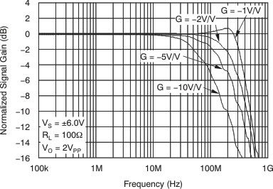
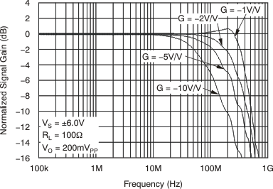
| Inverting Small-Signal Frequency Response | VO = 200 mVPP | Figure 4 |
| Inverting Large-Signal Frequency Response | VO = 2 VPP | Figure 5 |
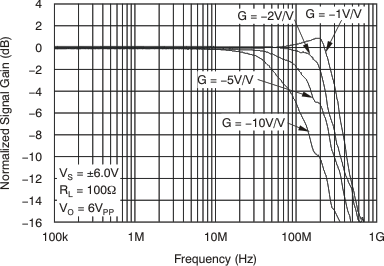
| Inverting Large-Signal Frequency Response | VO = 6 VPP | Figure 6 |
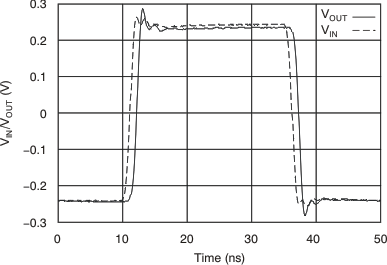
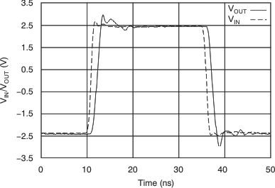
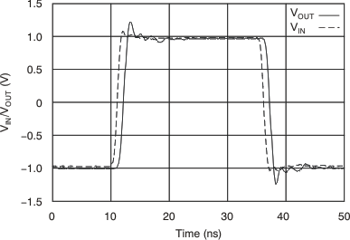
| Noninverting Transient Response | 0.5-V Step | Figure 7 |
| Noninverting Transient Response | 2-V Step | Figure 8 |
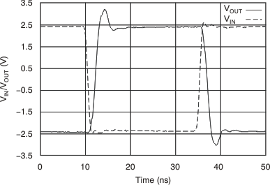
| Noninverting Transient Response | 5-V Step | Figure 9 |
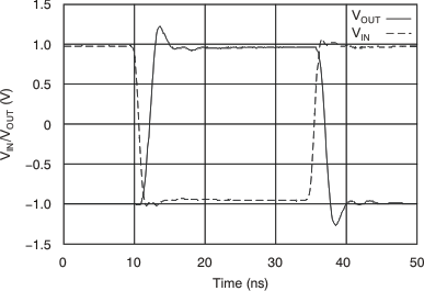
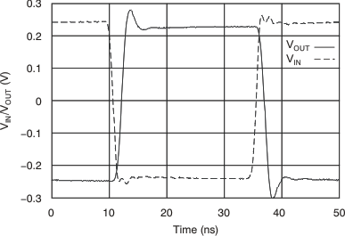
| Inverting Transient Response | 0.5-V Step | Figure 10 |
| Inverting Transient Response | 2-V Step | Figure 11 |
| Inverting Transient Response | 5-V Step | Figure 12 |
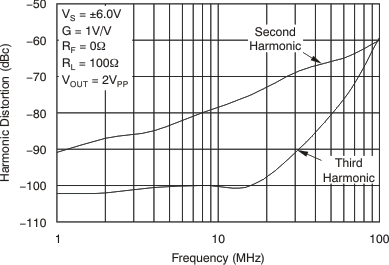
| Harmonic Distortion vs Frequency | Figure 13 | |
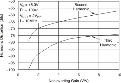
| Harmonic Distortion vs Noninverting Gain | Figure 14 | |
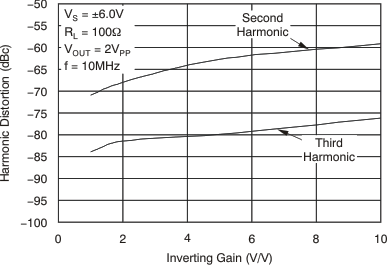
| Harmonic Distortion vs Inverting Gain | Figure 15 | |
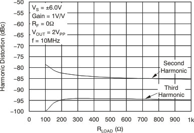
| Harmonic Distortion vs Load Resistance | Figure 16 | |
| Harmonic Distortion vs Output Voltage | Figure 17 | |
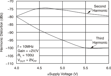
| Harmonic Distortion vs ±Supply Voltage | Figure 18 | |
| Two-Tone, Second- and Third-Order Intermodulation Distortion vs Frequency | Figure 19 | |
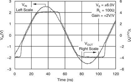
| Overdrive Recovery | Gain = 2 V/V | Figure 20 |
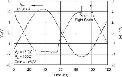
| Overdrive Recovery | Gain = –2 V/V | Figure 21 |
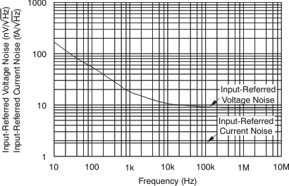
| Input-Referred Voltage Spectral Noise Density | Figure 22 | |
| Common-Mode Rejection Ratio and Power-Supply Rejection Ratio vs Frequency | Figure 23 | |
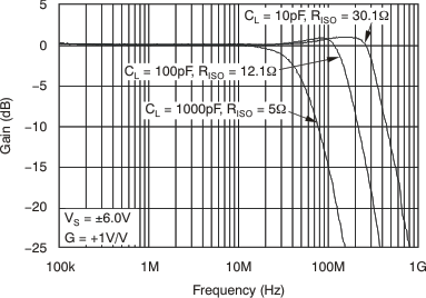
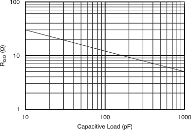
| Recommended RISO vs Capacitive Load | Figure 24 | |
| Frequency Response vs Capacitive Load | Figure 25 | |
| Open-Loop Gain and Phase | Figure 26 | |
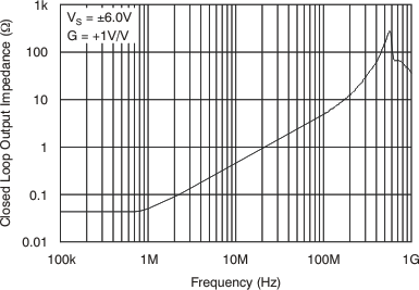
| Closed-Loop Output Impedance vs Frequency | Figure 27 | |
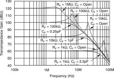
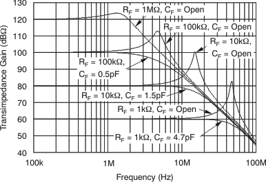
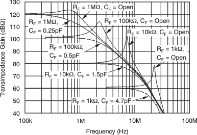
| Transimpedance Gain vs Frequency | CD = 10 pF | Figure 28 |
| Transimpedance Gain vs Frequency | CD = 22 pF | Figure 29 |
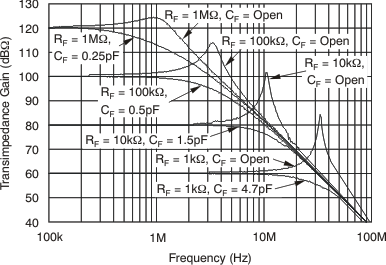
| Transimpedance Gain vs Frequency | CD = 47 pF | Figure 30 |
| Transimpedance Gain vs Frequency | CD = 100 pF | Figure 31 |
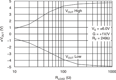
| Maximum/Minimum ±VOUT vs RLOAD | Figure 32 | |
| Slew Rate vs VOUT Step | Figure 33 | |
(VO = 2 VPP)
(RLOAD = 1 kΩ)
(CD = 100 pF)
(VO = 200 mVPP)
(VO = 6 VPP)
10 MHz
10 MHz
(RLOAD = 1 kΩ)
