SBOS223H December 2001 – October 2024 OPA690
PRODUCTION DATA
- 1
- 1 Features
- 2 Applications
- 3 Description
- 4 Device Comparison Table
- 5 Pin Configuration and Functions
-
6 Specifications
- 6.1 Absolute Maximum Ratings
- 6.2 ESD Ratings
- 6.3 Recommended Operating Conditions
- 6.4 Thermal Information
- 6.5 Electrical Characteristics OPA690IDBV, VS = ±5 V
- 6.6 Electrical Characteristics OPA690IDBV, VS = 5 V
- 6.7 Electrical Characteristics OPA690ID, VS = ±5 V
- 6.8 Electrical Characteristics OPA690ID, VS = 5 V
- 6.9 Typical Characteristics: OPA690IDBV, VS = ±5V
- 6.10 Typical Characteristics: OPA690IDBV, VS = 5V
- 6.11 Typical Characteristics: OPA690ID, VS = ±5V
- 6.12 Typical Characteristics: OPA690ID, VS = 5V
- 7 Detailed Description
- 8 Application and Implementation
- 9 Device and Documentation Support
- 10Revision History
- 11Mechanical, Packaging, and Orderable Information
Package Options
Refer to the PDF data sheet for device specific package drawings
Mechanical Data (Package|Pins)
- D|8
- DBV|6
Thermal pad, mechanical data (Package|Pins)
Orderable Information
7.3.2 Input and ESD Protection
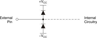
The OPA690 is built using a very high-speed complementary bipolar process. The internal junction breakdown voltages are relatively low for these very small geometry devices. These breakdowns are reflected in Section 6.1. All device pins are protected with internal ESD protection diodes to the power supplies. Figure 7-3 shows the internal ESD protection.
 Figure 7-3 Internal
ESD Protection
Figure 7-3 Internal
ESD ProtectionThese diodes also provide moderate protection to input overdrive voltages greater than the supplies. The protection diodes can typically support 10 mA of continuous current. Where higher currents are possible (for example, in systems with ±15-V supply parts driving into the OPA690), add current-limiting series resistors into the two inputs. Keep these resistor values as low as possible, because high values degrade both noise performance and frequency response.