SBOS223H December 2001 – October 2024 OPA690
PRODUCTION DATA
- 1
- 1 Features
- 2 Applications
- 3 Description
- 4 Device Comparison Table
- 5 Pin Configuration and Functions
-
6 Specifications
- 6.1 Absolute Maximum Ratings
- 6.2 ESD Ratings
- 6.3 Recommended Operating Conditions
- 6.4 Thermal Information
- 6.5 Electrical Characteristics OPA690IDBV, VS = ±5 V
- 6.6 Electrical Characteristics OPA690IDBV, VS = 5 V
- 6.7 Electrical Characteristics OPA690ID, VS = ±5 V
- 6.8 Electrical Characteristics OPA690ID, VS = 5 V
- 6.9 Typical Characteristics: OPA690IDBV, VS = ±5V
- 6.10 Typical Characteristics: OPA690IDBV, VS = 5V
- 6.11 Typical Characteristics: OPA690ID, VS = ±5V
- 6.12 Typical Characteristics: OPA690ID, VS = 5V
- 7 Detailed Description
- 8 Application and Implementation
- 9 Device and Documentation Support
- 10Revision History
- 11Mechanical, Packaging, and Orderable Information
Package Options
Refer to the PDF data sheet for device specific package drawings
Mechanical Data (Package|Pins)
- D|8
- DBV|6
Thermal pad, mechanical data (Package|Pins)
Orderable Information
8.2.1.2 Detailed Design Procedure
In this circuit, only one side of the complementary output drive signal is used. Figure 8-6 shows the signal output current connected into the virtual ground summing junction of the OPA690, which is set up as a transimpedance stage or I-V converter. The unused current output of the DAC is connected to ground. If the DAC requires that the outputs terminate to a compliance voltage other than ground for operation, the appropriate voltage level can be applied to the noninverting input of the OPA690. The dc gain for this circuit is equal to RF. At high frequencies, the DAC output capacitance produces a zero in the noise gain for the OPA690 that can cause peaking in the closed-loop frequency response. CF is added across RF to compensate for this noise gain peaking. To achieve a flat transimpedance frequency response, set the pole in the feedback network to Equation 6.
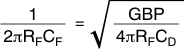
Equation 6 gives a closed-loop transimpedance bandwidth, f−3dB, of approximately Equation 7.
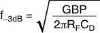
where
- GBP = gain bandwidth product (Hz) for the OPA690