SBOS223H December 2001 – October 2024 OPA690
PRODUCTION DATA
- 1
- 1 Features
- 2 Applications
- 3 Description
- 4 Device Comparison Table
- 5 Pin Configuration and Functions
-
6 Specifications
- 6.1 Absolute Maximum Ratings
- 6.2 ESD Ratings
- 6.3 Recommended Operating Conditions
- 6.4 Thermal Information
- 6.5 Electrical Characteristics OPA690IDBV, VS = ±5 V
- 6.6 Electrical Characteristics OPA690IDBV, VS = 5 V
- 6.7 Electrical Characteristics OPA690ID, VS = ±5 V
- 6.8 Electrical Characteristics OPA690ID, VS = 5 V
- 6.9 Typical Characteristics: OPA690IDBV, VS = ±5V
- 6.10 Typical Characteristics: OPA690IDBV, VS = 5V
- 6.11 Typical Characteristics: OPA690ID, VS = ±5V
- 6.12 Typical Characteristics: OPA690ID, VS = 5V
- 7 Detailed Description
- 8 Application and Implementation
- 9 Device and Documentation Support
- 10Revision History
- 11Mechanical, Packaging, and Orderable Information
Package Options
Refer to the PDF data sheet for device specific package drawings
Mechanical Data (Package|Pins)
- D|8
- DBV|6
Thermal pad, mechanical data (Package|Pins)
Orderable Information
7.3.1 Wideband Voltage-Feedback Operation
Typical differential input stages used for voltage-feedback op amps are designed to steer a fixed-bias current to the compensation capacitor, setting a limit to the achievable slew rate. The OPA690 uses a new input stage that places the transconductance element between two input buffers, using the output currents as the forward signal.
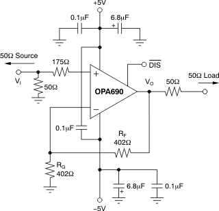
Figure 7-1 shows the dc-coupled, gain of 2 V/V, dual power-supply circuit configuration used as the basis of the Section 6.11. For test purposes, the input impedance is set to 50 Ω with a resistor to ground and the output impedance is set to 50 Ω with a series output resistor. Voltage swings reported in the specifications are taken directly at the input and output pins, while output powers (dBm) are at the matched 50-Ω load. For the circuit of Figure 7-1, the total effective load is 100 Ω || 804 Ω. The disable control line is typically left open to maintain normal amplifier operation. An additional resistor (175 Ω) is included in series with the noninverting input. Combined with the 25-Ω DC source resistance looking back towards the signal generator, this gives an input bias current canceling resistance that matches the 200-Ω source resistance seen at the inverting input (see Section 8.1.8). In addition to the usual power-supply decoupling capacitors to ground, a 0.1-µF capacitor is included between the two power-supply pins. In practical printed-circuit board (PCB) layouts, this optional-added capacitor typically improves the 2nd-harmonic distortion performance.
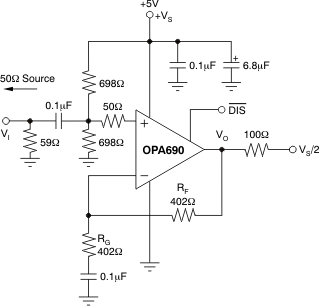
Figure 7-2 shows the AC-coupled, gain of 2, single-supply circuit configuration which is the basis of the 5 V and Section 6.12. Although not a rail-to-rail design, the OPA690 requires minimal input and output voltage headroom compared to other very wideband voltage-feedback op amps. The device delivers a 3-VPP output swing on a single 5-V supply with > 120-MHz bandwidth. The key requirement of broadband single-supply operation is to maintain input and output signal swings within the useable voltage ranges at both the input and the output. The circuit of Figure 7-2 establishes an input midpoint bias using a simple resistive divider from the 5‑V supply (two 698-Ω resistors). The input signal is then ac-coupled into the midpoint voltage bias. The input voltage can swing to within 1.5 V of either supply pin, giving a 2-VPP input signal range centered between the supply pins. The input impedance matching resistor (59 Ω) used for testing is adjusted to give a 50-Ω input load when the parallel combination of the biasing divider network is included.
 Figure 7-1 DC-Coupled, G = 2 V/V,
Bipolar-Supply Specification and Test Circuit
 Figure 7-2 AC-Coupled, G = 2 V/V,
Single-Supply Specification and Test Circuit
Figure 7-2 AC-Coupled, G = 2 V/V,
Single-Supply Specification and Test CircuitAgain, an additional resistor (50 Ω in this case) is included directly in series with the noninverting input. This minimum recommended value provides part of the dc source resistance matching for the noninverting input bias current. The additional resistor is also used to form a simple parasitic pole to roll off the frequency response at very high frequencies (> 500 MHz) using the input parasitic capacitance to form a band-limiting pole. The gain resistor (RG) is ac-coupled, giving the circuit a dc gain of 1, which puts the input dc bias voltage (2.5 V) at the output as well. The output voltage can swing to within 1 V of either supply pin while delivering > 100-mA output current. A demanding 100-Ω load to a midpoint bias is used in this characterization circuit. The new output stage circuit used in the OPA690 can deliver large output currents into this midpoint load with minimal crossover distortion .