SBOS293I December 2003 – October 2024 OPA695
PRODUCTION DATA
- 1
- 1 Features
- 2 Applications
- 3 Description
- 4 Pin Configuration and Functions
-
5 Specifications
- 5.1 Absolute Maximum Ratings
- 5.2 ESD Ratings
- 5.3 Recommended Operating Conditions
- 5.4 Thermal Information
- 5.5 Electrical Characteristics VS = ±5 V, OPA695ID, OPA695IDBV
- 5.6 Electrical Characteristics VS = 5 V, OPA695ID, OPA695IDBV
- 5.7 Electrical Characteristics VS = ±5 V, OPA695IDGK
- 5.8 Electrical Characteristics VS = 5 V, OPA695IDGK
- 5.9 Typical Characteristics: VS = ±5 V, OPA695IDBV, OPA695ID
- 5.10 Typical Characteristics: VS = 5 V, OPA695IDBV, OPA695ID
- 5.11 Typical Characteristics: VS = ±5 V, OPA695IDGK
- 5.12 Typical Characteristics: VS = 5 V, OPA695IDGK
- 6 Detailed Description
- 7 Application and Implementation
- 8 Device and Documentation Support
- 9 Revision History
- 10Mechanical, Packaging, and Orderable Information
Package Options
Refer to the PDF data sheet for device specific package drawings
Mechanical Data (Package|Pins)
- D|8
- DBV|6
- DGK|8
Thermal pad, mechanical data (Package|Pins)
Orderable Information
6.3.2 Input and ESD Protection
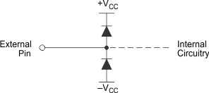
The OPA695 is built using a very high-speed, complementary bipolar process. The internal junction breakdown voltages are relatively low for these small geometry devices. These breakdowns are reflected in the Absolute Maximum Ratings, where an absolute maximum ±6.5-V supply is reported. All device pins have limited ESD protection using internal diodes to the power supplies, as shown in Figure 6-3.
These diodes also provide moderate protection to input overdrive voltages above the supplies. The protection diodes can typically support 10-mA continuous current. Where higher currents are possible (for example, in systems with ±15-V supply parts driving into the OPA695), add current-limiting series resistors into the two inputs. Keep these resistor values as low as possible because high values degrade both noise performance and frequency response.
 Figure 6-3 Internal ESD
Protection