SBOS293I December 2003 – October 2024 OPA695
PRODUCTION DATA
- 1
- 1 Features
- 2 Applications
- 3 Description
- 4 Pin Configuration and Functions
-
5 Specifications
- 5.1 Absolute Maximum Ratings
- 5.2 ESD Ratings
- 5.3 Recommended Operating Conditions
- 5.4 Thermal Information
- 5.5 Electrical Characteristics VS = ±5 V, OPA695ID, OPA695IDBV
- 5.6 Electrical Characteristics VS = 5 V, OPA695ID, OPA695IDBV
- 5.7 Electrical Characteristics VS = ±5 V, OPA695IDGK
- 5.8 Electrical Characteristics VS = 5 V, OPA695IDGK
- 5.9 Typical Characteristics: VS = ±5 V, OPA695IDBV, OPA695ID
- 5.10 Typical Characteristics: VS = 5 V, OPA695IDBV, OPA695ID
- 5.11 Typical Characteristics: VS = ±5 V, OPA695IDGK
- 5.12 Typical Characteristics: VS = 5 V, OPA695IDGK
- 6 Detailed Description
- 7 Application and Implementation
- 8 Device and Documentation Support
- 9 Revision History
- 10Mechanical, Packaging, and Orderable Information
Package Options
Refer to the PDF data sheet for device specific package drawings
Mechanical Data (Package|Pins)
- D|8
- DBV|6
- DGK|8
Thermal pad, mechanical data (Package|Pins)
Orderable Information
7.1.1.1 Setting Resistor Values to Optimize Bandwidth
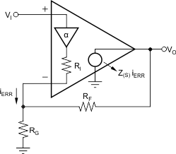
A current-feedback operational amplifier such as the OPA695 can hold an almost constant bandwidth over signal gain settings with the proper adjustment of the external resistor values. Section 5.9 shows this feature. The small-signal bandwidth decreases only slightly with increasing gain. These curves also show that the feedback resistor has been changed for each gain setting. The absolute values of RF on the inverting side of the circuit for a current-feedback operational amplifier can be treated as frequency response compensation elements, whereas the ratios of RF and RG set the signal gain. Figure 7-1 shows the analysis circuit for the OPA695 small-signal frequency response.
The key elements of this current feedback operational amplifier model are:
- α ⇒ Buffer gain from the noninverting input to the inverting input.
- RI ⇒ Buffer output impedance
- iERR ⇒ Feedback error current signal
- Z(s) ⇒ Frequency-dependent, open-loop transimpedance gain from iERR to VO
 Figure 7-1 Current-Feedback Transfer Function Analysis
Circuit
Figure 7-1 Current-Feedback Transfer Function Analysis
CircuitA current-feedback operational amplifier senses an error current in the inverting node (as opposed to a differential input error voltage for a voltage-feedback operational amplifier) and passes this on to the output through an internal frequency-dependent transimpedance gain. Section 5.9 show this open-loop transimpedance response. This is analogous to the open-loop voltage gain curve for a voltage-feedback operational amplifier. Refer to the training videos shown in TI Precision Labs for further understanding on the CFA operating theory
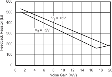
The values for RF versus gain shown in Figure 7-2 are approximately equal to the values used to generate the typical characteristics and give a good starting point for designs where bandwidth optimization is desired.
 Figure 7-2 Recommended Feedback Resistor vs Noise
Gain