SBOS293I December 2003 – October 2024 OPA695
PRODUCTION DATA
- 1
- 1 Features
- 2 Applications
- 3 Description
- 4 Pin Configuration and Functions
-
5 Specifications
- 5.1 Absolute Maximum Ratings
- 5.2 ESD Ratings
- 5.3 Recommended Operating Conditions
- 5.4 Thermal Information
- 5.5 Electrical Characteristics VS = ±5 V, OPA695ID, OPA695IDBV
- 5.6 Electrical Characteristics VS = 5 V, OPA695ID, OPA695IDBV
- 5.7 Electrical Characteristics VS = ±5 V, OPA695IDGK
- 5.8 Electrical Characteristics VS = 5 V, OPA695IDGK
- 5.9 Typical Characteristics: VS = ±5 V, OPA695IDBV, OPA695ID
- 5.10 Typical Characteristics: VS = 5 V, OPA695IDBV, OPA695ID
- 5.11 Typical Characteristics: VS = ±5 V, OPA695IDGK
- 5.12 Typical Characteristics: VS = 5 V, OPA695IDGK
- 6 Detailed Description
- 7 Application and Implementation
- 8 Device and Documentation Support
- 9 Revision History
- 10Mechanical, Packaging, and Orderable Information
Package Options
Refer to the PDF data sheet for device specific package drawings
Mechanical Data (Package|Pins)
- D|8
- DBV|6
- DGK|8
Thermal pad, mechanical data (Package|Pins)
Orderable Information
7.1.3.2 Arbitrary Waveform Driver
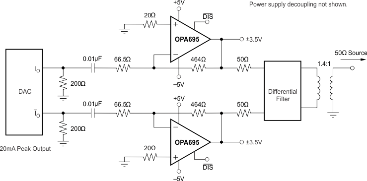
The OPA695 can be used as the output stage for moderate output power arbitrary waveform driver applications. Driving out through a series 50-Ω matching resistor into a 50-Ω matched load allows up to a 4.0-VPP swing at the matched load (15 dBm) when operating the OPA695 on a ±5-V power supply. This level of power is available for gains of either ±8 V/V with a flat response through 100 MHz. When interfacing directly from a complementary current output DAC, consider the circuit of Figure 7-7, modified for the peak output currents of the particular DAC being considered. Where purely ac-coupled output signals are required from a complementary current output DAC, consider a push-pull output stage using the circuit of Figure 7-7. The resistor values here have been calculated for a 20-mA peak output current DAC, which produces up to a 5-VPP swing at the matched load (18 dBm). This approach gives higher power at the load, with lower 2nd-harmonic distortion.
For a 20-mA peak output current DAC, the midscale current of 10 mA gives a 2-V dc output common-mode operating voltage, due to the 200-Ω resistor to ground at the outputs. The total ac impedance at each output is 50 Ω, giving a ±0.5-V swing around this 2-V common-mode voltage for the DAC. These resistors also act as a current divider, sending 75% of the DAC output current through the feedback resistor (464 Ω). The blocking capacitor references the OPA695 output voltage to ground, and turns the unipolar DAC output current into a bipolar swing of 0.75 × 20 mA × 464 Ω = 7 VPP at each amplifier output. Each output is exactly 180° out-of-phase from the other, producing double 7 VPP into the matching resistors. To limit the peak output current and improve distortion, the circuit of Figure 7-7 is set up with a 1.4:1 step-down transformer. This reflects the 50-Ω load to be 100 Ω at the primary side of the transformer. For the maximum 14-VPP swing across the outputs of the two amplifiers, the matching resistors drop this to 7 VPP at the input of the transformer, then down to 5-VPP maximum at the 50-Ω load at the output of the transformer. This step-down approach reduces the peak output current to 14 VP/(200 Ω) = 70 mA.
 Figure 7-7 High Power, Wideband AC-Coupled Arbitrary Waveform Driver