SBOS799E August 2019 – August 2024 OPA810
PRODUCTION DATA
- 1
- 1 Features
- 2 Applications
- 3 Description
- 4 Device Comparison Table
- 5 Pin Configuration and Functions
-
6 Specifications
- 6.1 Absolute Maximum Ratings
- 6.2 ESD Ratings
- 6.3 Recommended Operating Conditions
- 6.4 Thermal Information
- 6.5 Electrical Characteristics: 10 V
- 6.6 Electrical Characteristics: 24 V
- 6.7 Electrical Characteristics: 5 V
- 6.8 Typical Characteristics: VS = 10 V
- 6.9 Typical Characteristics: VS = 24 V
- 6.10 Typical Characteristics: VS = 5 V
- 6.11 Typical Characteristics: ±2.375-V to ±12-V Split Supply
- 7 Detailed Description
- 8 Application and Implementation
- 9 Device and Documentation Support
- 10Revision History
- 11Mechanical, Packaging, and Orderable Information
Package Options
Refer to the PDF data sheet for device specific package drawings
Mechanical Data (Package|Pins)
- D|8
- DBV|5
- DCK|5
Thermal pad, mechanical data (Package|Pins)
Orderable Information
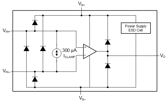
7.3.2 ESD Protection
As Figure 7-2 shows, all device pins are protected with internal ESD protection diodes to the power supplies. These diodes provide moderate protection to input overdrive voltages above the supplies. The protection diodes can typically support 10-mA continuous input and output currents. The differential input clamps only limit the bias current when the input common-mode voltages are within the supply voltage range, whereas current-limiting series resistors must be added at the inputs if common-mode voltages higher than the supply voltages are possible. Keep these resistor values as low as possible because using high values degrades noise performance and frequency response.
 Figure 7-2 Internal ESD Protection