SBOS799E August   2019  – August 2024 OPA810

PRODUCTION DATA  

  1.   1
  2. Features
  3. Applications
  4. Description
  5. Device Comparison Table
  6. Pin Configuration and Functions
  7. Specifications
    1. 6.1  Absolute Maximum Ratings
    2. 6.2  ESD Ratings
    3. 6.3  Recommended Operating Conditions
    4. 6.4  Thermal Information
    5. 6.5  Electrical Characteristics: 10 V
    6. 6.6  Electrical Characteristics: 24 V
    7. 6.7  Electrical Characteristics: 5 V
    8. 6.8  Typical Characteristics: VS = 10 V
    9. 6.9  Typical Characteristics: VS = 24 V
    10. 6.10 Typical Characteristics: VS = 5 V
    11. 6.11 Typical Characteristics: ±2.375-V to ±12-V Split Supply
  8. Detailed Description
    1. 7.1 Overview
    2. 7.2 Functional Block Diagram
    3. 7.3 Feature Description
      1. 7.3.1 OPA810 Architecture
      2. 7.3.2 ESD Protection
    4. 7.4 Device Functional Modes
      1. 7.4.1 Split-Supply Operation (±2.375 V to ±13.5 V)
      2. 7.4.2 Single-Supply Operation (4.75 V to 27 V)
  9. Application and Implementation
    1. 8.1 Application Information
      1. 8.1.1 Amplifier Gain Configurations
      2. 8.1.2 Selection of Feedback Resistors
      3. 8.1.3 Noise Analysis and the Effect of Resistor Elements on Total Noise
    2. 8.2 Typical Applications
      1. 8.2.1 Transimpedance Amplifier
        1. 8.2.1.1 Design Requirements
        2. 8.2.1.2 Detailed Design Procedure
        3. 8.2.1.3 Application Curves
      2. 8.2.2 High-Z Input Data Acquisition Front-End
      3. 8.2.3 Multichannel Sensor Interface
    3. 8.3 Power Supply Recommendations
    4. 8.4 Layout
      1. 8.4.1 Layout Guidelines
        1. 8.4.1.1 Thermal Considerations
      2. 8.4.2 Layout Example
  10. Device and Documentation Support
    1. 9.1 Third-Party Products Disclaimer
    2. 9.2 Documentation Support
      1. 9.2.1 Related Documentation
    3. 9.3 Receiving Notification of Documentation Updates
    4. 9.4 Support Resources
    5. 9.5 Trademarks
    6. 9.6 Electrostatic Discharge Caution
    7. 9.7 Glossary
  11. 10Revision History
  12. 11Mechanical, Packaging, and Orderable Information

Package Options

Refer to the PDF data sheet for device specific package drawings

Mechanical Data (Package|Pins)
  • D|8
  • DBV|5
  • DCK|5
Thermal pad, mechanical data (Package|Pins)
Orderable Information

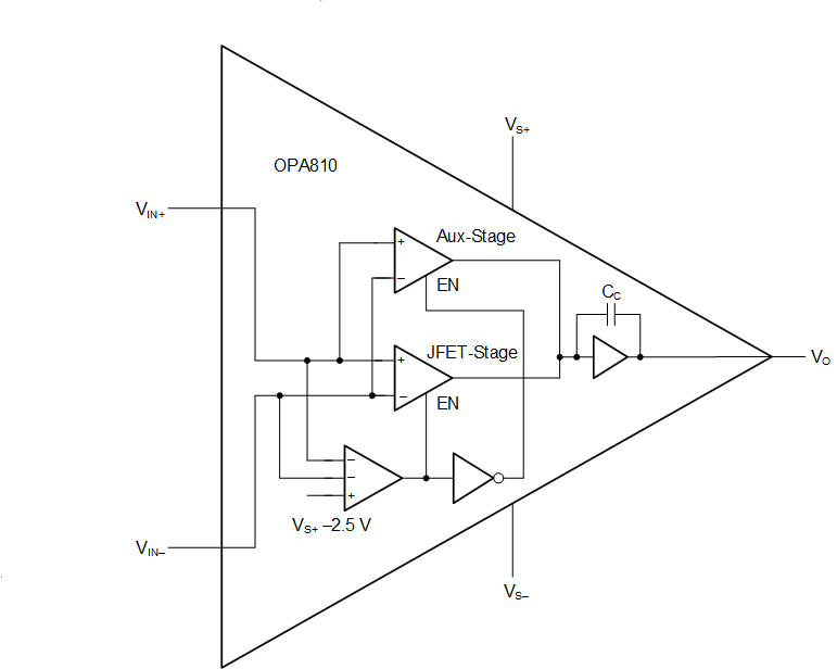
Functional Block Diagram

OPA810