SBOS799E August 2019 – August 2024 OPA810
PRODUCTION DATA
- 1
- 1 Features
- 2 Applications
- 3 Description
- 4 Device Comparison Table
- 5 Pin Configuration and Functions
-
6 Specifications
- 6.1 Absolute Maximum Ratings
- 6.2 ESD Ratings
- 6.3 Recommended Operating Conditions
- 6.4 Thermal Information
- 6.5 Electrical Characteristics: 10 V
- 6.6 Electrical Characteristics: 24 V
- 6.7 Electrical Characteristics: 5 V
- 6.8 Typical Characteristics: VS = 10 V
- 6.9 Typical Characteristics: VS = 24 V
- 6.10 Typical Characteristics: VS = 5 V
- 6.11 Typical Characteristics: ±2.375-V to ±12-V Split Supply
- 7 Detailed Description
- 8 Application and Implementation
- 9 Device and Documentation Support
- 10Revision History
- 11Mechanical, Packaging, and Orderable Information
Package Options
Refer to the PDF data sheet for device specific package drawings
Mechanical Data (Package|Pins)
- D|8
- DBV|5
- DCK|5
Thermal pad, mechanical data (Package|Pins)
Orderable Information
3 Description
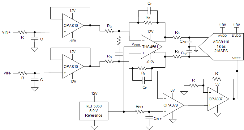
The OPA810 is a single-channel, field-effect transistor (FET) input, voltage-feedback operational amplifier with bias current in the picoampere (pA) range. The OPA810 is unity-gain stable with a small-signal, unity-gain bandwidth of 140MHz, and offers excellent dc precision and dynamic ac performance at a low quiescent current (IQ) of 3.7mA per channel. The OPA810 is fabricated on Texas Instruments' proprietary, high-speed SiGe BiCMOS process and achieves significant performance improvements over comparable FET-input amplifiers at similar levels of quiescent power. With a gain-bandwidth product (GBWP) of 70MHz, slew rate of 200V/µs, and low-noise voltage of 6.3nV/√Hz, the OPA810 is designed for use in a wide range of high-fidelity data-acquisition and signal-processing applications.
The OPA810 features rail-to-rail inputs and outputs, and delivers 75mA of linear output current designed to drive optoelectronic components and analog-to-digital converter (ADC) inputs or buffer digital-to-analog converter (DAC) outputs into heavy loads.
The OPA810 is specified over the extended industrial temperature range of –40°C to +125°C. The OPA2810 is a dual-channel variant of the OPA810, available in 8-pin SOIC, SOT-23, and VSSOP packages.
| PART NUMBER | PACKAGE(1) | PACKAGE SIZE(2) |
|---|---|---|
| OPA810 | D (SOIC, 8) | 4.9mm × 6mm |
| DBV (SOT-23, 5) | 2.9mm × 2.8mm | |
| DCK (SC70, 5) | 2mm × 2.1mm |
 Hi-Z-Input, Data-Acquisition Front End